background image

High-Level Data Link Control (HDLC)

15-10

Am186™CC/CH/CU Microcontrollers User’s Manual

Remote Loopback Mode: To enable Remote Loopback mode, set the LOOPR bit in 
the HxCON register to 1. Remote Loopback disables the transmitter and echoes the 
data received at the serial input out to the serial output. The receiver operates normally 
in this mode.

Local Loopback Mode: To enable Local Loopback mode, set the LOOPL bit in the 
HxCON register to 1. Local Loopback mode disconnects the serial input and connects 
the serial output to the receiver input. The serial output can operate in three-state, open 
drain, or totem pole mode.

CRC Type: The algorithm for CRC generation and checking can be CRC-CCIT, CRC-16, 
or CRC-32. Specify the CRC type in the CRCTYPE field of the HxCON register.

Time Slot Assigner (TSA): Each HDLC channel is tightly coupled with a TSA, which 
can operate in either multiplexed or nonmultiplexed (pass-through) mode. In multiplexed 
mode, the TXCLK input becomes the synchronization input and the TSA connects the 
receive clock to the transmit clock. In multiplexed mode, the TSA controller determines 
when to enable and disable the HDLC clock. It also allows the user to reduce the number 
of bits transmitted in a single 8-bit time slot. This reduction allows the transmission of 
data from 64 Kbit/s down to 8 Kbit/s in 8 Kbit/s decrements. This feature allows the HDLC 
channel to be used for LAP-D and reduced data mode LAP-B transmissions such as 
56 Kbit/s.

15.5.4

HDLC Transmitter

The transmitter functions include:

Opening flag transmission

Data transparency (via zero insertion)

Generation and transmission of the CRC frame-check-sequence characters (if enabled)

Transmission of the closing flag.

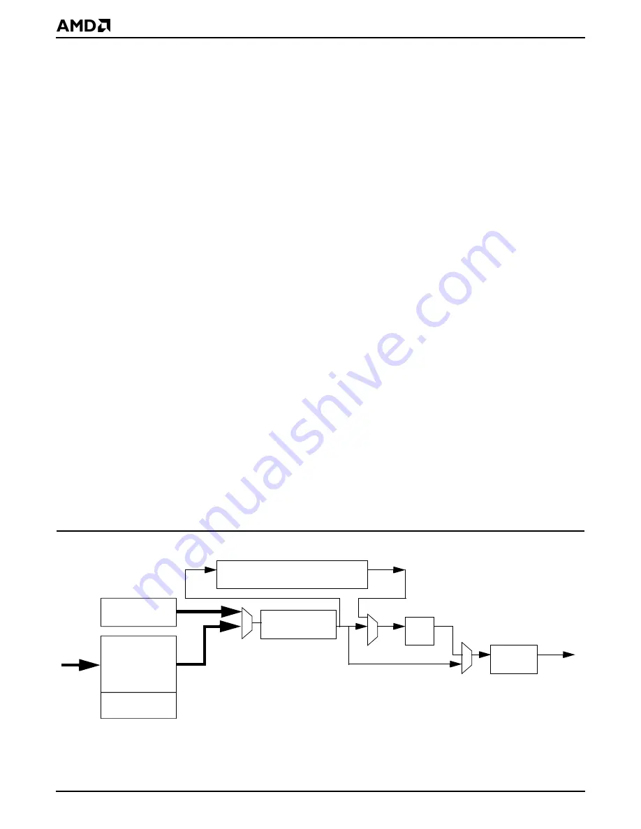
Figure 15-3 illustrates the block diagram for the transmitter.

Note: The HDLC transmitter requires at least one byte of data surrounded by flags: the 
start flag, one byte of data, and the end flag. A 2-byte CRC with no data also constitutes a 
valid transmission. The HDLC receiver can receive only frames two bytes or longer.

Figure 15-3

HDLC Transmitter Block Diagram 

Flag/Abort

Generator

CRC Generator (16- or 32-bit)

Zero

Insert

Transmit

Transparent Mode Path

Parallel-to-Serial

Shift Register

FIFO

Serial

From
CPU

output

NRZ/NRZI

Encoder

End-of-Frame 

Tag

Содержание Am186 CC

Страница 1: ...Am186 CC CH CU Microcontrollers User s Manual Order 21914B...

Страница 2: ...ication neither states nor implies any representations or warranties of any kind including but not limited to any implied warranty of merchantability or fitness for a particular purpose AMD products a...

Страница 3: ...n E86 and Comm86 products access the AMD home page at www amd com and follow the Embedded Processors link These pages provide information on upcoming product releases overviews of existing products in...

Страница 4: ...iv Am186 CC CH CU Microcontrollers User s Manual...

Страница 5: ...HDLC Channels and TSAs 1 7 1 4 2 3 General Circuit Interface 1 8 1 4 2 4 SmartDMA Channels 1 8 1 4 2 5 Asynchronous Serial Ports 1 9 1 4 2 6 Synchronous Serial Port 1 9 1 4 3 System Peripherals 1 9 1...

Страница 6: ...7 Clock Control 3 32 3 7 1 Clock Features 3 32 3 7 2 PLL Bypass Mode 3 34 3 8 Hardware Related Considerations 3 34 3 9 Comparison To Other Devices 3 34 3 10 Initialization 3 34 CHAPTER 4 EMULATOR SUPP...

Страница 7: ...CS and Non LCS 5 9 5 5 5 3 PCS I O Space 5 9 5 5 6 Programming Ready Signals and Wait States 5 10 5 5 7 Chip Select Timing 5 10 5 5 8 Hardware Related Considerations 5 10 5 5 9 Software Related Consid...

Страница 8: ...sters Used 7 18 7 5 6 Nonmaskable Interrupts 7 18 7 5 6 1 Software Interrupts 7 19 7 5 6 2 Divide Error Exception Interrupt Type 00h 7 19 7 5 6 3 Trace Interrupt Interrupt Type 01h 7 19 7 5 6 4 Nonmas...

Страница 9: ...Design 9 2 9 4 Registers 9 5 9 5 Operation 9 5 9 5 1 Usage 9 5 9 5 2 Defining the PIO Signal as Input or Output 9 5 9 5 3 Driving Data on the PIO 9 6 9 5 4 Using PIOs as Open Drain Outputs 9 6 9 5 5...

Страница 10: ...sters 13 3 13 5 Operation 13 4 13 5 1 Usage 13 4 13 5 1 1 Transmit 13 5 13 5 1 2 Receive 13 6 13 5 1 3 Autobaud Mode High Speed UART Only 13 7 13 5 2 Data 13 8 13 5 2 1 Data Overflow 13 8 13 5 2 2 Add...

Страница 11: ...5 2 2 Programmed I O Interface 15 8 15 5 3 General HDLC Options 15 9 15 5 4 HDLC Transmitter 15 10 15 5 5 HDLC Receiver 15 14 15 5 6 HDLC and SmartDMA 15 18 15 5 6 1 HDLC Transmitter 15 18 15 5 6 2 HD...

Страница 12: ...l Operation 17 19 17 5 8 Interrupts 17 19 17 5 9 Software Related Considerations 17 20 17 5 10 Comparison to Other Devices 17 20 17 6 Initialization 17 20 CHAPTER 18 UNIVERSAL SERIAL BUS USB 18 1 18 1...

Страница 13: ...18 5 9 2 Commands Handled by the USB Peripheral Controller Hardware 18 27 18 5 10 Command Protocol 18 28 18 5 10 1 Data Transfer Using the Control Endpoint 18 29 18 5 10 2 Control Endpoint Interrupts...

Страница 14: ...zed General Purpose DMA Transfers 8 19 Figure 8 6 SmartDMA Channel Descriptor Ring Example 8 29 Figure 8 7 SmartDMA Channel Memory Management 8 30 Figure 8 8 SmartDMA Transmit Channel Flow Diagram 8 3...

Страница 15: ...6 4 ISDN PCM System Application Example 16 5 Figure 16 5 ISDN Basic Rate GCI Application Am186CC Communications Controller 16 10 Figure 16 6 Programmable Frame Sync 16 13 Figure 16 7 Converted GCI Clo...

Страница 16: ...le 7 5 Interrupt Channel Sources 7 17 Table 8 1 DMA Multiplexed Signals 8 4 Table 8 2 DMA Controller Register Summary 8 4 Table 8 3 Am186CC Communications Controller DMA Channel Use 8 8 Table 8 4 Am18...

Страница 17: ...GCI Multiplexed Signals Same as Table 15 1 17 3 Table 17 2 GCI Register Summary 17 5 Table 17 3 GCI Signals 17 13 Table 17 4 Converted GCI Signals 17 14 Table 17 5 TIC Bus Bits 17 16 Table 18 1 USB Mu...

Страница 18: ...Table of Contents xviii Am186 CC CH CU Microcontrollers User s Manual...

Страница 19: ...4 is intended for computer software and hardware engineers and system architects who are designing or are considering designing systems based on one of these controllers Overview of this Manual This m...

Страница 20: ...chronous Serial Ports UARTs describes how to use the UART and High Speed UART for asynchronous serial data transfer Chapter 14 Synchronous Serial Port SSI discusses how to use the SSI synchronous seri...

Страница 21: ...Communications Controller to an AMD SLAC Device Using the Enhanced SSI order 21921 application note describes how to connect these two devices The same techniques can be used to connect the Am186CC mi...

Страница 22: ...signal internal reset A reset initiated by the watchdog timer see Chapter 11 Watchdog Timer system reset Assertion of the RESOUT signal to reset external peripherals An external reset always causes a...

Страница 23: ...mediately following a heading indicates that the information under that heading up to the next heading applies only to the indicated controllers Icons that appear other than at the beginning of the ch...

Страница 24: ...Introduction xxiv Am186 CC CH CU Microcontrollers User s Manual...

Страница 25: ...trollers A customer development platform board for silicon evaluation and software development is available Reference designs under development include a low end router with Integrated Services Digita...

Страница 26: ...roller that is targeted towards cost sensitive applications such as linecards and digital phones The Am186CH HDLC microcontroller is pin compatible with the Am186CC microcontroller and offers many of...

Страница 27: ...6CC microcontroller and offers many of the same features yet the Am186CU USB microcontroller provides a cost effective solution for USB devices that do not need GCI or HDLC It includes the following d...

Страница 28: ...Highway Interface GCI IOM 2 Interface USB Peripheral Controller SmartDMA Channels 8 4 pair 4 2 pair 4 2 pair General Purpose DMA Channels 4 4 4 High Speed UART UART Synchronous Serial Interface SSI I...

Страница 29: ...IOs Serial Interface SSI Timers 3 System Peripherals Memory Peripherals CC Smart DMA 4 General Purpose DMA 4 Physical Interface Raw DCE PCM Serial Communications Peripherals TSA TSA Glueless Interface...

Страница 30: ...ports the use of SmartDMA with the serial interfaces The Am186CU USB microcontroller supports four serial interfaces a USB peripheral controller two UARTs and an SSI In addition it supports the use of...

Страница 31: ...mon PCM highway or other time division multiplexed TDM bus with the other channels or to work in some combination The Am186CC microcontroller supports raw DCE PCM highway and GCI interfaces The Am186C...

Страница 32: ...troller also allows conversion of the GCI clock and GCI frame sync into a format usable by PCM codecs allowing the use of PCM codecs directly with GCI IOM 2 transceivers Additional GCI features includ...

Страница 33: ...Using this protocol the microcontroller sends a command byte to the attached device and then follows that byte with either a read or write of a byte of data The SSI port consists of three I O pins an...

Страница 34: ...of the Am186CC CH CU microcontrollers provides 48 user programmable input output signals PIOs In the Am186CC microcontroller each of these signals shares a pin with at least one alternate function In...

Страница 35: ...y mapped and I O mapped external peripherals and memory devices The bus interface accesses the internal peripherals through the PCB The bus interface features programmable bus sizing separate byte wri...

Страница 36: ...s in either memory or I O space The six memory chip selects can address three memory ranges Each peripheral chip select addresses a 256 byte block offset from a programmable base address The microcont...

Страница 37: ...Embedded x86 processors have long been used in the industrial control market These applications often require a robust high performance processor solution with the capability to easily communicate wi...

Страница 38: ...Architectural Overview 1 14 Am186 CC CH CU Microcontrollers User s Manual Figure 1 4 ISDN Terminal Adapter Figure 1 5 ISDN to Ethernet Low End Router CC CC...

Страница 39: ...Architectural Overview Am186 CC CH CU Microcontrollers User s Manual 1 15 Figure 1 6 32 Channel Linecard CH CC...

Страница 40: ...Architectural Overview 1 16 Am186 CC CH CU Microcontrollers User s Manual...

Страница 41: ...an access peripheral registers This section briefly describes these processor and peripheral registers For detailed information on the microcontroller peripheral registers see the Am186 CC CH CU Micro...

Страница 42: ...rs Four 16 bit special purpose registers CS DS ES and SS select at any given time the segments of memory that are immediately addressable for code CS data DS and ES and stack SS memory Status and Cont...

Страница 43: ...rupt vector This flag is cleared when the processor takes a hardware interrupt or a trace interrupt by using the CLI instruction For more information about hardware and software interrupts see Chapter...

Страница 44: ...t to 20FCh which maps the PCB to start at FC00h in I O space This places the RELOC register at FFFEh Appendix A Register Summary provides a summary of PCB registers in offset order including default a...

Страница 45: ...of registers with their bit field names and offset addresses see Appendix A Register Summary The Am186 CC CH CU Microcontrollers Register Set Manual order 21916 de scribes these registers in detail T...

Страница 46: ...lculating the offset value see Addressing Modes on page 2 9 For more information about CS DS ES and SS see Segments on page 2 7 In addition to 1 Mbyte of memory space the Am186CC microcontroller provi...

Страница 47: ...s the default location for all instructions All code must be executed from the code segment 3 Stack Segment SS The processor uses the SS register to perform operations that involve the stack such as p...

Страница 48: ...resentation Packed BCD A packed byte representation of two decimal digits 0 9 Each nibble four bits of the byte contains one digit Pointer A 16 bit or 32 bit quantity composed of a 16 bit offset compo...

Страница 49: ...ix The offset also called the effective address is calculated by summing any combination of the following three address elements Displacement An 8 bit or 16 bit immediate value contained in the instru...

Страница 50: ...t and the contents of a base register BX or BP Indexed Mode The operand offset is the sum of an 8 bit or 16 bit displacement and the contents of an index register SI or DI Based Indexed Mode The opera...

Страница 51: ...CAS1 MCS2 128 CAS0 MCS3 129 RAS1 PIO5 DRAM CAS0 128 SRAM MCS2 PIO CAS1 127 MCS1 RAS0 131 LCS RAS1 129 MCS3 PIO5 Synchronous Communications Interfaces DCE Channel A DCE_RXD_A 118 PCM Channel A PCM_RXD_...

Страница 52: ...PIO44 PCM Channel D PCM_RXD_D 158 DCE Channel D DCE_RXD_D Low Speed UART RXD_U High Speed UART PIO PIO26 PCM_TXD_D 159 DCE_TXD_D TXD_U PIO20 PCM_CLK_D 156 DCE_RCLK_D RTR_U PIO25 PCM_FSC_D 157 DCE_TCL...

Страница 53: ...PIO10 2 SDEN PIO11 3 SCLK PIO12 4 SDATA PIO13 5 PCS0 PIO14 6 PCS1 PIO15 16 WR PIO16 25 RXD_HU PIO17 123 DCE_CTS_A PCM_TSC_A PIO18 122 DCE_RTR_A PIO19 145 INT6 PIO20 159 TXD_U DCE_TXD_D PCM_TXD_D PIO2...

Страница 54: ...PCS7 PIO32 11 PCS6 PIO33 19 ALE PIO34 20 BHE PIO35 15 SRDY PIO36 138 DCE_RXD_B PCM_RXD_B PIO37 139 DCE_TXD_B PCM_TXD_B PIO38 137 DCE_CTS_B PCM_TSC_B PIO39 136 DCE_RTR_B PIO40 135 DCE_RCLK_B PCM_CLK_B...

Страница 55: ...tiated by the watchdog timer System reset Resets the microcontroller the CPU plus the internal peripherals as well as any external peripherals connected to RESOUT An external reset always causes a sys...

Страница 56: ...an place configuration information on the AD bus using weak external pullup or pulldown resistors or using an external driver that is enabled during reset The processor does not drive the AD bus durin...

Страница 57: ...ONCE mode Otherwise the controller operates normally In ONCE mode all pins are three stated and remain in that state until a subsequent reset occurs To guarantee that the controller does not inadverte...

Страница 58: ...atchdog timer page 3 14 Reserved page 3 16 Power and ground page 3 16 Debug support page 3 17 Chip selects page 3 17 DRAM page 3 19 Interrupts page 3 19 Programmable I O PIOs page 3 21 Programmable ti...

Страница 59: ...CPU plus the internal peripherals as well as any external peripherals connected to RESOUT An external reset always causes a system reset an internal reset can optionally cause a system reset signal Re...

Страница 60: ...ed see the ADEN pin description in Table 3 5 on page 3 7 During a reset condition the address and data bus is three stated with pulldowns and during a bus hold it is three stated In addition during a...

Страница 61: ...stated during the t2 t3 and t4 phases The value driven on the A bus is undefined during a refresh cycle For this reason the A0 signal cannot be used in place of the AD0 signal to determine refresh cy...

Страница 62: ...edge is asserted to indicate to an external bus master that the microcontroller has relinquished control of the local bus When an external bus master requests control of thelocalbus by assertingHOLD t...

Страница 63: ...minating the HOLD input For more information see the HLDA pin description above RD O Read Strobe indicates to the system that the microcontroller is performing a memory or I O read cycle RD is guarant...

Страница 64: ...th AD15 AD8 WHB is the logical AND of BHE and WR This pin is three stated with a pullup during bus hold or reset conditions WLB is asserted with AD7 AD0 WLB is the logical AND of AD0 and WR This pin i...

Страница 65: ...ded with a Schmitt trigger to facilitate power on RES generation via a resistor capacitor RC network RESOUT O ResetOut indicates that the microcontroller is beingreset either externally or internally...

Страница 66: ...6 RSVD_80 RSVD_81 RSVD_101 UTXDPLS RSVD_102 UTXDMNS RSVD_103 UXVOE RSVD_104 UXVRCV RSVD_116 RSVD_117 RSVD_118 RSVD_119 POWER AND GROUND VCC 15 16 STI Digital Power Supply pins supply power 3 3 0 3 V t...

Страница 67: ...lup resistor during bus hold or reset conditions MCS0 MCS1 MCS2 MCS3 UCSX8 PIO4 CAS1 CAS0 RAS1 PIO5 O Midrange Memory Chip Selects 0 3 indicate to the system that a memory access is in progress to the...

Страница 68: ...ultiplexed AD address and data bus timing PCS1 PIO14 USBSEL2 PCS2 PCS3 PCS4 PIO3 CLKSEL2 PCS5 PIO2 PCS6 PIO32 PCS7 PIO31 UCS ONCE O Upper Memory Chip Select indicates to the system that a memory acces...

Страница 69: ...signal to the upper DRAM bank INTERRUPTS INT5 INT0 STI Maskable Interrupt Requests 0 8 indicate to the microcontroller that an external interrupt request has occurred If the individual pin is not mask...

Страница 70: ...cleared when the processor takes the interrupt disabling the maskable interrupt sources However if maskable interrupts are re enabled by software in the NMI interrupt service routine for example via t...

Страница 71: ...re multiplexed with alternate signals that can be used by emulators PIO8 PIO15 PIO33 PIO34 and PIO35 Consider any emulator requirements for the alternate signals before using these pins as PIOs PROGRA...

Страница 72: ...controller CTS_U DCE_TCLK_D PCM_FSC_D PIO24 STI Clear To Send UART provides the Clear to Send signal from the asynchronous serial port when hardware flow control is enabled for the port The CTS_U sign...

Страница 73: ...the microcontroller and a slave device SDATA PIO12 B Serial Data is used to transmit and receive data between the microcontroller and a slave device on the synchronous serial interface SDEN PIO10 O Se...

Страница 74: ...to the channel B DCE interface that an external serial interface is ready to receive data DCE_CTS_B and DCE_RTR_B provide the handshaking for the channel B DCE interface DCE_RTR_B PIO39 O DCE Ready t...

Страница 75: ...hannel D indicates to the channel D DCE interface that an external serial interface is ready to receive data DCE_CTS_D and DCE_RTR_D provide the handshaking for DCE Channel D DCE_RTR_D RTR_HU High Spe...

Страница 76: ...peration PCM_CLK_C is the single transmit and receive data clock input pin for the channel C PCM Highway interface PCM_CLK_C becomes a clock source output when the GCI to PCM Highway clock and frame s...

Страница 77: ...SERIAL BUS USB UDMNS UDPLS USBD USBD STI STI USB External Transceiver Gated Differential Plus and USB ExternalTransceiverGatedDifferentialMinusareinputsfrom the external USB transceiver used to detect...

Страница 78: ...e Data Strobe DEN DS and Data Transmit Receive signal DT R provided to support an external data bus transceiver and to support a bus interface to 68xxx style peripherals Support for the Reset Configur...

Страница 79: ...tem With DRAM Figure 3 2 Typical Microcontroller Memory System With SRAM CAS0 CAS1 RAS0 Flash Memory 4 Mbit DRAM MA8 MA0 WE OE Data CAS0 CAS1 RAS0 WR A19 A0 UCS AD15 AD0 RD WE Address CS Data OE x8 or...

Страница 80: ...dress disable is in effect the number of signals that assert on the bus during all normal bus cycles to the associated address space is reduced thus decreasing power consumption reducing processor swi...

Страница 81: ...ompletes the bus cycle in progress It then relinquishes control of the bus to the external bus master by asserting HLDA and floating S2 S0 AD15 AD0 S6 TMROUT1 and TMROUT0 During HOLD internal pullups...

Страница 82: ...e system clock 3 7 1 Clock Features The microcontroller includes the following clock features and characteristics Figure 3 3 illustrates the clocks For detailed information on the clocks see the data...

Страница 83: ...ontroller supports the following clock frequencies HDLC DCE mode supports clocks up to 10 MHz HDLC PCM mode supports clocks up to 10 MHz HDLC GCI mode supports a 1 536 MHz clock input System clock mus...

Страница 84: ...on reset pinstraps are not resampled during a watchdog timer reset If the external reset RES signal is asserted while the watchdog timer is performing a watchdog timer reset the external reset takes p...

Страница 85: ...an external and an internal reset selects full HDLC with flow control for external interface D and sets HDLC Channel C for raw DCE or PCM Highway mode On an external reset the following also occurs Pi...

Страница 86: ...System Overview 3 36 Am186 CC CH CU Microcontrollers User s Manual...

Страница 87: ...nals It is important that these pins not be multiplexed in such a way as to compromise the emulator operation Fortunately several pin functions can be successfully multiplexed Emulators generally do n...

Страница 88: ...f the A19 A0 address pins Therefore these pins are always available for emulation 4 3 2 2 AD15 AD0 The Am186CC CH CU microcontrollers do not multiplex any AD15 AD0 address data pins with other functio...

Страница 89: ...low half of the data bus and the high half of the data bus Although it is possible to snoop all events that determine the memory width chip select pulldowns during reset and UMCS LMCS and MPCS regist...

Страница 90: ...is being placed in ONCE modeand thereset signal has a very slow rise time Emulator vendors solve this problem by providing a reset signal with a fast rise time The hardware designer must use this emul...

Страница 91: ...e may use the WR signal to determine when writes occur This prevents the use of WR as a PIO when using the emulator 4 3 2 24 WLB See UCSX8 and WLB 4 3 2 25 WR See WHB and WR 4 3 3 Hardware Related Con...

Страница 92: ...Emulator Support 4 6 Am186 CC CH CU Microcontrollers User s Manual...

Страница 93: ...wait states inserted in the bus cycle Although most memory and peripheral devices can be accessed with three or fewer wait states some slower devices cannot This feature allows devices to use external...

Страница 94: ...als when enabled either disable or alter any other functions that use the same pin For diagrams of some example applications see Chapter 3 System Overview Internal UCS CS DRAM Registers PCB_AD Write D...

Страница 95: ...Select Register Summary Offset Register Mnemonic Register Name Description 3A0h UMCS Upper Memory Chip Select Programs the lower boundary of the Upper Memory Chip Select UCS Also supports DRAM 3A2h LM...

Страница 96: ...A bit DRAM enable UDEN bit Data bus width USIZ bit External Ready mode R2 bit Wait state value R1 and R0 bits UCS is active on reset To use the Lower Memory Chip Select LCS configure the following LMC...

Страница 97: ...th the LB bit field in the UMCS register The block size must be a multiple of 64 Kbyte 5 5 2 2 LCS The LCS chip select is for the bottom of the 1 Mbyte memory address space The lower boundary is 00000...

Страница 98: ...e in the CPU s I O space bits BA 19 16 are forced to 0 by hardware as the upper bound of the CPU s I O space is 64 Kbytes The MS bit in the MPCS register determines whether PCS chip selects are mapped...

Страница 99: ...gnal can select the en tire middle chip select range when MCS Only mode is enabled Also the MCS3 MCS1 pins are multiplexed with programmable I O pins To enable their DRAM functionality the PIO Mode an...

Страница 100: ...erlapping see Selecting DRAM Using the Chip Selects on page 5 7 In systems where the chip selects must overlap the chip selects whose assertions overlap must have the same configuration for ready exte...

Страница 101: ...o a 16 bit space through software and not the reverse If the system does a watchdog timer reset this bit reverts to the value sampled on UCSX8 during the last external reset The UCSX8 signal has a wea...

Страница 102: ...mpletes after six cycles four cycles plus two wait states If external ready is not asserted during the first wait cycle the access is extended until ready is asserted which is followed by one more wai...

Страница 103: ...al reset the following occurs The microcontroller begins fetching and executing instructions starting at memory location FFFF0h so upper memory is typically used as instruction memory To facilitate th...

Страница 104: ...elects are not enabled until software writes to both the MMCS and MPCS registers Data bus widths are set as follows LCS is 16 bits wide Non UCS and non LCS memory MCS PCS and the remaining memory that...

Страница 105: ...The Row Address Strobe RAS and Column Address Strobe CAS signals latch the row and column addresses inside the DRAM To support DRAM the Am186CC CH CU microcontrollers each have a fully integrated DRAM...

Страница 106: ...s of some example applications see Chapter 3 System Overview Table 6 1 DRAM Multiplexed Signals Signal Multiplexed Signal s Default Signal Function CAS0 MCS2 MCS2 Column address strobes CAS1 MCS1 MCS1...

Страница 107: ...s not load the new value into the refresh counter until the current counter value has reached 0 3 Set the EN bit of the EDRAM register to 1 to enable DRAM refresh 6 5 2 DRAM Supported The Am186CC CH C...

Страница 108: ...ad or write The RAS0 signal controls the lower bank of DRAM which starts at 00000h in the address map and is bounded by the ending address selected with the UB bit field in the LMCS register The RAS1...

Страница 109: ...r greater number of wait states than the DRAM In the case of an overlap the bus width during PCS accesses is 16 bits 6 5 5 DRAM Refresh 6 5 5 1 DRAM Refresh Cycle When DRAM refresh is enabled it opera...

Страница 110: ...o use for refresh time intervals to be placed into the RC bit field of the CDRAM register TheAm186CC CH CU microcontrollerssupportDRAMswithaCAS before RAS refreshing scheme A refresh is generated base...

Страница 111: ...llowing occurs The value of the CDRAM register becomes 0000h setting the DRAM refresh period to 0 The value of the EDRAM register becomes 0000h clearing and disabling the refresh counter The UDEN bit...

Страница 112: ...DRAM Controller 6 8 Am186 CC CH CU Microcontrollers User s Manual...

Страница 113: ...nonmaskable interrupt NMI a trace interrupt and software interrupts and exceptions The interrupt controller supports the maskable interrupt sources through the use of 15 channels To make this possible...

Страница 114: ...internal NMI is generated by the microcontroller s watchdog timer For more information on the watchdog timer see Chapter 11 Watchdog Timer A trace interrupt is generated with the trace flag TF bit in...

Страница 115: ...alter any other functions that use the same pin For diagrams of some example applications see Chapter 3 System Overview Watchdog Timer Interrupt Controller Execution Unit External NMI Internal NMI INT...

Страница 116: ...CU Microcontrollers Register Set Manual order 21916 Table 7 1 Interrupt Multiplexed Signals Signal Multiplexed Signal s Default Signal Function INT0 INT0 Maskable interrupt requests INT1 INT1 INT2 INT...

Страница 117: ...e bit of an interrupt that is currently in service 322h POLL Poll Indicates the interrupt type of the highest priority pending interrupt 324h POLLST Poll Status Copy of the POLL register Reading the P...

Страница 118: ...MR0 even though they had different vectors This happened because for all other sources the vector number was identical with the EOI type In the Am186CC CH CU microcontrollers any of the three vector n...

Страница 119: ...ring the external interrupts INT8 INT0 and the PIO interrupts clear the IF flag in the FLAGS register with the CLI instruction However most of the microcontroller s internal interrupts can be safely c...

Страница 120: ...hen those two types have the same level of programmable priority Programmable Priority Each channel has eight levels of programmable priority which are set in the Channel Control CHxCON register Progr...

Страница 121: ...source has a corresponding interrupt type Each interrupt type has a four byte vector available in the interrupt vector table The interrupt vector table is located in the 1024 bytes from 00000h to 003F...

Страница 122: ...an interrupt is being serviced is that the processor reads the interrupt vector table 7 5 3 4 End of Interrupt EOI Software must write to the End of Interrupt EOI register to reset the CHx bit in the...

Страница 123: ...g software exceptions After the trace interrupt and the NMI watchdog timer interrupt the remaining software exceptions are mutually exclusive and can only occur one at a time so there is no further pr...

Страница 124: ...1C2 Unused Opcode Exception 06h 18h Undefined Opcodes 1C2 ESC Opcode Exception 07h 1ch ESC Opcodes 1C2 Maskable Interrupts Timer 0 08h 20h Channel 0 2A Timer 1 09h 24h Channel 0 2B Timer 2 0Ah 28h Cha...

Страница 125: ...nized 5 If the interrupt is recognized the controller generates an interrupt request to the execution unit 6 If the IF flag in the FLAGS register is set the execution unit recognizes the request Other...

Страница 126: ...executing NMI routine assuming it meets the criteria outlined above DMA activity may be re enabled by clearing the DHLT bit but this could increase the number of cycles required to complete the NMI r...

Страница 127: ...d only by interrupts of equal or higher priority than the in service interrupt When an interrupt service routine completes software must reset the proper in service bit by writing the EOI type to the...

Страница 128: ...r 1 X Timer 2 X High Speed UART X UART X HDLC_A X HDLC_B X HDLC_C X HDLC_D X GCI X SDMA0 X SDMA1 X SDMA2 X SDMA3 X GP DMA0 X GP DMA1 X GP DMA2 X GP DMA3 X USB X INT0 X INT1 X X INT2 X X INT3 X X INT4...

Страница 129: ...nnel 14 a register individually masks on or off the signals serviced by this channel so that individual control of interrupt sources is possible 2 For a complete description of Pulse Width Demodulatio...

Страница 130: ...ters used to control interrupts see the Am186 CC CH CU Microcontrollers Register Set Manual order 21916 In addition bits 8 and 9 in the FLAGS register relate to interrupt operation Bit 8 of the FLAGS...

Страница 131: ...see Chapter 2 Configuration Basics 7 5 6 4 Nonmaskable Interrupt Interrupt Type 02h An NMI can be generated internally or externally An internal NMI is generated with the watchdog timer For more infor...

Страница 132: ...g Therefore a watchdog timer generated NMI can interrupt or be interrupted by an externally generated NMI For more information about the watchdog timer NMI see Considerations for NMI Software Interrup...

Страница 133: ...are active The Interrupt Request REQST Interrupt Status INTSTS and Shared Request SHREQ registers are cleared indicating there are no pending interrupts The DMA Halt DMAHLT register is cleared so DMA...

Страница 134: ...Interrupts 7 22 Am186 CC CH CU Microcontrollers User s Manual...

Страница 135: ...eral to memory The Am186CC microcontroller provides a total of 12 DMA channels eight SmartDMA channels and four general purpose DMA channels Four of the SmartDMA channels two pairs are dedicated for u...

Страница 136: ...red to or from even or odd addresses on the Am186CC CH CU microcontrollers Two bus cycles a minimum of eight clocks are necessary for each general purpose DMA data transaction For word transfers both...

Страница 137: ...0 TX_DMA3 0 20 Bit GP DMA SDMA SDMA Control Arbiter DMA Generator Cycle DRQ Select DRQ1 DRQ0 Control Bus TC Bus DST SRC ADDR Bus Select DRQ11 DRQ0 RX_DMA3 0 RX_DMA3 0 Bus Request Bus Grant PCB Interfa...

Страница 138: ...except the GDxCON0 and GDxCON1 registers can be modified or altered during any DMA activity Any changes made to these registers are reflected immediately in DMA operation Table 8 1 DMA Multiplexed Sig...

Страница 139: ...Ch GD1TC General Purpose DMA1 TransferCount 120h GD2CON0 General Purpose DMA2 Control 0 Behaves the same as General Purpose DMA0 registers but for DMA Channel 2 122h GD2CON1 General Purpose DMA2 Contr...

Страница 140: ...ring high address bits 19 16 for SmartDMA Channel 0 14Ah SD0STAT SmartDMA0 Status Indicates the status of SmartDMA Channel 0 14Ch SD0CBD SmartDMA0 Current Buffer Descriptor Indicates the buffer descr...

Страница 141: ...nel 0 registers but for SmartDMA Channel 2 172h SD2TRCAL SmartDMA2 Transmit Ring Count Address Low 174h SD2TRAH SmartDMA2 Transmit Ring Address High 176h SD2RRCAL SmartDMA2 Receive Ring Count Address...

Страница 142: ...UT endpoint1 Notes 1 For SmartDMA channels 2 and 3 the transmit and receive cannot be assigned to different pe ripherals For example if SmartDMA Channel 2 receive is assigned to USB data endpoint A th...

Страница 143: ...wer priority channels and can effectively hold off lower priority DMA requests for multiple transfers When two DMA requests of the same programmed priority have transfers pending they alternate transf...

Страница 144: ...re 8 2 Source Versus Destination Synchronization 8 5 4 DMA Acknowledge TheAm186CC CH CU microcontrollersdonotprovideanexplicit DMA acknowledgesignal Because both source and destination registers are m...

Страница 145: ...low control information such as XONs and XOFFs may not be seen as quickly To alleviate this condition transmission can be done without using DMA e g from within the same interrupt routine or byprogram...

Страница 146: ...channels on the Am186CC CH CU microcontrollers are completely interchangeable and the register sets are identical From the programmer s point of view a DMA cycle proceeds as follows 1 The DMA channel...

Страница 147: ...g conditions suspend general purpose DMA transfers Deassertion of DRQ A bus hold condition A refresh cycle by an NMI watchdog timer interrupt A pending DMA request of equal or higher priority The DHLT...

Страница 148: ...te the transfer when the count reaches zero The GDxTC register wraps back to its maximum value and continues decrementing If the current transfer is an unsynchronized transfer DMA terminates when the...

Страница 149: ...remented or decremented by 2 an increment by one causes unpredictable results Byte transfers can be incremented or decremented by 1 or 2 When a byte transfer is incremented or decremented by 2 the hig...

Страница 150: ...rt data register SPTXD SPRXD HSPTXD or HSPRXD Note Using a DMA channel with a UART deactivates the corresponding external DMA request signal For DMA to the UART or High Speed UART specify the followin...

Страница 151: ...ynchronized Unsynchronized Transfers For unsynchronized DMA transfers the DRQ signal is internally tied High When initiated an unsynchronized DMA transfer begins immediately and consumes all bus cycle...

Страница 152: ...synchronization the device receiving the data asserts the DMA request Figure 8 5 shows a typical destination synchronized DMA transfer The DMA controller does not sample the DRQ line for a channel unt...

Страница 153: ...least four clocks before the end of the transfer If more transfers are not required a source synchronized transfer allows the source device at least three clock cycles from the time it is acknowledged...

Страница 154: ...addresses until the programmed buffer length is reached at which point the address is reset to its initial value data is never written outside the programmed buffer space Circular buffers can be progr...

Страница 155: ...he buffer is freed and the next buffer is set up to be transferred out using DMA Reception is more difficult because it is not always known up front exactly how long the incoming message is Even if th...

Страница 156: ...rovement available by improving UART transmission Table 8 9 gives typical register values for using circular buffers with the UARTs Table 8 9 Example Register Settings for UARTs and Circular Buffers G...

Страница 157: ...errupt handler If a multitasking system is used an attempt to write too much data to the buffer should write as much as possible and then block the task performing the write until additional space is...

Страница 158: ...ut not the TC bit in the GDxCON0 register This causes the DMA to interrupt when there is room buffer size minus high water mark in the buffer and an XOFF can be sent The value chosen for the high wate...

Страница 159: ...DMA activity to stop until an interrupt task services the exception The decision of whether to set or clear the EXDRD bit depends on the intended usage If the target baud rate is high relative to syst...

Страница 160: ...can support either the third or fourth HDLC channel or USB endpoints A B C or D The four SmartDMA channels two pairs SDMA0 and SDMA1 in the Am186CH HDLC microcontroller support the two on board HDLC...

Страница 161: ...the Am186CC microcontroller SmartDMA Channel 2 and SmartDMA Channel 3 provide the DSEL bit in the SDxCON control register for selecting between the HDLC and USB request source The address of the perip...

Страница 162: ...16 32 64 or 128 descriptors Even when the ring size is set to 1 that entry is still interpreted as a descriptor not as the memory buffer itself Each entry in the descriptor ring is composed of a 20 bi...

Страница 163: ...get the buffer it would be in poll mode and wait until the buffer is available The SmartDMA controller clears the OWN bit when it releases control of the buffer Some systems may need to have DMA trans...

Страница 164: ...acket The channel has already transmitted the data from buffer 1 and is currently processing buffer 2 While packet x is being transmitted software is writing data to buffer 4 for transmission of the n...

Страница 165: ...g any DRQs In addition because the SmartDMA channel works off of requests from the device it is always safe to enable the DMA before the device Enabling the device before the DMA may result in data lo...

Страница 166: ...as interrupted Add Data Buffers to the Transmit Descriptor Ring To place a data buffer in an entry in the transmit buffer descriptor ring 1 Find the first buffer descriptor for which the OWN bit is cl...

Страница 167: ...bling the Receive Channel To enable a SmartDMA receive channel software must perform the following tasks 1 Create the receive buffer descriptor ring 2 Program the interrupt channel and configure the S...

Страница 168: ...buffer address a Program the LADR bits in Word 0 to the low order 16 address bits of the data buffer pointed to by the descriptor b Program the HADR bits in Word 1 to the high order eight address bits...

Страница 169: ...ot exist on the Am186CC CH CU microcontrollers 20 bit address but are provided for LANCE compatibility 2 Set to 1 the OWN bit in Word 1 to indicate the descriptor entry is owned by the SmartDMA channe...

Страница 170: ...ts to acquire the next buffer The transmit channel releases the current buffer by clearing the OWN bit unless the TXS0 bit is set It then advances to the next descriptor in the ring If the OWN bit is...

Страница 171: ...iptor the SmartDMA controller loads the address of the buffer into an internal receive address register The length of the buffer is also read from the descriptor and programmed into an internal termin...

Страница 172: ...mation from the device and writes it to the descriptor Theend of packet bit is set in the descriptor and the OWN bit is cleared If RXS0 is set the EOP bit is set but the OWN bit not cleared 7 The rece...

Страница 173: ...the first buffer of the packet or the SmartDMA channel skips over this descriptor and polls the next descriptor s until both the OWN and STP bits are set 8 ENP The ENP End of Packet bit indicates tha...

Страница 174: ...yclic Redundancy Check Error bit indicates When HDLC is the requesting source the current frame has a CRC error When USB is the requesting source one of the following errors occurred If the USB endpoi...

Страница 175: ...bits of the data buffer pointed to by this descriptor The highest four bits of the address must be set to 0000b These address bits do not exist in the microcontroller s 20 bit address space but are pr...

Страница 176: ...on transmit descriptor rings because any system that wants to be interrupted after there are no more buffers in the ring to send out can rely on the TBUI interrupt see the description below TBUI and R...

Страница 177: ...ch descriptor points to a portion of the physical buffer and the DMA can be started at any arbitrary point by adjusting the descriptors starting addresses and lengths and setting the SDxCBD registers...

Страница 178: ...Manual 8 6 INITIALIZATION On both an internal and external reset the following occurs All the general purpose DMA and SmartDMA channel registers are cleared to 0 Any DMA transfer in progress is aborte...

Страница 179: ...a PIO an appropriate default value for the signal is sent to the associated device rather than the value on the pin A PIO can be configured to operate as an input or output with or without internal p...

Страница 180: ...er any other functions that use the same pin The table also shows which register bit programs the pin to be the PIO or alternate function Alternate Function Data Out Data Out PIO Direction Register Wr...

Страница 181: ...PIO13 PCS0 PCS0 input with pullup PIOMODE0 13 PIO14 PCS1 PCS1 input with pullup PIOMODE0 14 PIO15 WR WR input with pullup PIOMODE0 15 PIO16 RXD_HU PIO16 input with pullup PIOMODE1 0 PIO17 DCE_CTS_A P...

Страница 182: ..._B PIO38 input with pullup PIOMODE2 6 PIO39 DCE_RTR_B PIO39 input with pullup PIOMODE2 7 PIO40 DCE_RCLK_B PCM_CLK_B PIO40 input with pullup PIOMODE2 8 PIO41 DCE_TCLK_B PCM_FSC_B PIO41 input with pullu...

Страница 183: ...er Summary Offset Register Mnemonic Register Name Description 3C0h PIOMODE0 PIO Mode 0 Set PIO15 PIO0 to PIO or alternate function and as input or output see Table 9 3 3C2h PIODIR0 PIO Direction 0 3C4...

Страница 184: ...Set or PIO Clear registers returns the last value written by software in the corresponding PIO Data register including changes made via the PIO Set and PIO Clear registers This enables software to rea...

Страница 185: ...he bits needed and writing the register 9 5 8 Comparison to Other Devices The PIO registers are similar to previous Am186 controller implementations The PIO Mode PIO Direction and PIO Data registers b...

Страница 186: ...Programmable I O Signals 9 8 Am186 CC CH CU Microcontrollers User s Manual...

Страница 187: ...one fourth of the CPU clock frequency every fourth CPU clock tick The source clock for Timers 0 and 1 can be the timer input pin Timer 2 or one fourth of the CPU clock The microcontroller also provide...

Страница 188: ...PIO6 TMRIN0 Timer inputs PIO27 PIO27 TMRIN1 PIO0 PIO0 TMROUT0 Timer outputs PIO28 PIO28 TMROUT1 PIO1 PIO1 Table 10 2 Programmable Timers Register Summary Offset Register Mnemonic Register Name Descri...

Страница 189: ...nfigured for alternate operation These pins are configured as PIOs at external and internal reset For more information see Chapter 9 Programmable I O Signals 10 5 2 Timer 2 When enabled Timer 2 increm...

Страница 190: ...imers 0 and 1 provide two maximum count compare registers TxCMPA and TxCMPB The setting of the ALT alternate compare bit determines whether one or both of these compare registers are used When ALT is...

Страница 191: ...clears the EN Enable bit and the timer is disabled If the CONT bit is set the timer remains enabled and performs the next compare against TxCMPA Because the comparison is done after the count is incre...

Страница 192: ...not support analog to digital conversion Figure 10 1 on page 10 1 shows the routing of signals when pulse width demodulation is either enabled or disabled The waveform for PWD mode is input on the INT...

Страница 193: ...tion of each phase of the input signal should not exceed 4 TxCMPA processor clocks because the timer increments every fourth processor clock in this configuration To extend the maximum measurable dura...

Страница 194: ...rs For more information see the Timer Mode and Control registers in the Am186 CC CH CU Microcontrollers Register Set Manual order 21916 10 5 9 Comparison to Other Devices The programmable timers are 1...

Страница 195: ...ing an external reset and can be pulled Low during an internal reset The watchdog timer provides a method to regain control when a system has failed due to a software error or to the failure of an ext...

Страница 196: ...state The watchdog timer must function in all cases where either the software or external devices have failed to respond appropriately The watchdog timer has incorporated several features to ensure t...

Страница 197: ...yed sequence of AAAAh followed by 5555h to the WDTCON register address As with the write key any number of processor cycles including memory and I O reads and writes can be inserted between the two ha...

Страница 198: ...timer time out occurred Software should clear this bit so that subsequent external NMIs are not confused with watchdog timer NMIs What actions are taken are system dependent however possible actions...

Страница 199: ...set as long as these writes have the enable bit cleared When a write is detected with the enable bit set the control register becomes read only except for the NMI Flag NMIFLAG bit and the Reset Flag R...

Страница 200: ...Watchdog Timer 11 6 Am186 CC CH CU Microcontrollers User s Manual...

Страница 201: ...HDLC channels on the Am186CC and Am186CH microcontrollers provide 8 bit element byte or character or frame full duplex synchronous serial data transmission The clock is provided by the Time Slot Assig...

Страница 202: ...SC_B PIO38 DCE_RTR_B 136 PIO39 DCE Channel C DCE_RXD_C 153 PCM Channel C PCM_RXD_C GCI to PCM Con version PIO PIO42 DCE_TXD_C 154 PCM_TXD_C PIO43 DCE_RCLK_C 150 PCM_CLK_C PCM_CLK_C PIO22 DCE_TCLK_C 14...

Страница 203: ...rocontroller This application uses three HDLC channels multiplexed off external interface A the High Speed UART port for a serial AT modem connection to the host PC and the debug UART port on external...

Страница 204: ...g or console UART RawDCE External interface D RawDCE External interface C RawDCE External interface B RawDCE External interface A CC UARTs High Speed UART UART External Interface HDLC Channels Channel...

Страница 205: ...ces B and C are used as PIOS External interface A TSA Channels Channel D Channel C Channel B Channel A SSI SSI to POTS ICs USB Connection to host PC GCI External Interface CC UARTs High Speed UART UAR...

Страница 206: ...synchronized While this addresses the timing problem the receiver must also be able to determine the beginning and end of a block of data To achieve this each block of data has some start and end bit...

Страница 207: ...des Polled mode disables interrupts and the DMA controller The software loops on a status register reading in all wait situations In interrupt mode interrupts are enabled Software does other tasks whi...

Страница 208: ...ata in either direction but not both at the same time a full duplex system can send data in both directions simultaneously In the Am186CC CH CU microcontrollers the SSI supports half duplex transfers...

Страница 209: ...read and write modes that allow word wide DMA transfers Multidrop protocol 9 data bit support Use of processor clock or external clock signal for generation of baud clock Full duplex operation One or...

Страница 210: ...s specific to the High Speed UART are marked High Speed UART Only UART signal names begin with SP High Speed UART signal names begin with HSP Signals for both start with H SP Figure 13 1 UARTs Block D...

Страница 211: ...rs Register Set Manual order 21916 In addition to these registers the ITF4 bit field in the System Configuration SYSCON register of the Am186CC microcontroller configures external interface 4 for the...

Страница 212: ...terruptsbasedonconditionofstatus bits 268h HSPTXD High Speed Serial Port Transmit Data Provides data to transmitter 26Ah HSPRXD High Speed Serial Port Receive Data Contains data read over serial line...

Страница 213: ...must be set in both registers for the interrupt to be taken If software disables an interrupt in H SPIMSK it can still read the status from the H SPSTAT register 5 Set the applicable configuration op...

Страница 214: ...Speed Serial Port Character Match HSPM0 HSPM1 and HSPM2 registers with the characters to be matched Each match register contains two character fields Note that 00h is a valid value so if you do not wa...

Страница 215: ...er to 0 6 Set the applicable configuration options in the HSPCON0 register interrupts breaks CTS RTR hardware flow control parity odd even or none address bit enable number of data bits in serial fram...

Страница 216: ...PCON0 register The TXD line is always held High between frames In asynchronous serial communication an idle line can be differentiated from an active receive line by the absence of start bits in the d...

Страница 217: ...s for encoded discrete commands e g sending a hang up command to a modem What the code is used for and how is determined by software To use the address bit in the microcontroller the ABEN and D7 bits...

Страница 218: ...r some conditions such as when the DMA interface is being used it may be useful forsoftwareto be able to examine the received characterwithoutaffecting the status register or removing the data from th...

Страница 219: ...s should be disabled FIFOs are initialized to the empty condition on reset For subsequent transfers the transmit FIFO and the receive FIFO should be flushed by software by setting the TFLUSH and RFLUS...

Страница 220: ...rdware and must be cleared by software The serial port can be configured to generate an interrupt based on serial port status Each status bit is individually maskable If an interrupting status conditi...

Страница 221: ...U and RXD_HU for the High Speed UART and two flow control signals CTS_U and RTR_U for the UART and CTS_HU and RTR_HU for the High Speed UART Hardware flow control is enabled when the FC bit in the H S...

Страница 222: ...lock or the UCLK input signal The possible clock configurations are shown graphically in Figure 13 6 The XTRN bit in the H SPCON1 register selects the clock source The baud clock is generated by divid...

Страница 223: ...Dh 0 9208d 23F8h 0 10000d 2710h 0 10417d 28B1h 0 600 2500d 09C4h 0 2604d 0A2Ch 0 4167d 1047h 0 4604d 11FCh 0 5000d 1388h 0 5208d 1458h 0 1200 1250d 04E2h 0 1302d 0516h 0 2083d 0823h 0 2302d 08FEh 0 25...

Страница 224: ...ting the Baud Rate Automatically High Speed UART Only The High Speed UART supports automatic baud rate detection autobaud by setting the ABAUD bit in the HSPCON1 register to 1 When in autobaud mode th...

Страница 225: ...Speed Serial Port Autobaud registers are provided for this enhancement HSPAB0 HSPAB1 HSPAB2 and HSPAB3 Each register contains a divisor value and a threshold value The HSPAB3 register must contain the...

Страница 226: ...n to the baud divisor register by dividing by 16 as shown in Programming the Baud Rate on page 13 15 The configuration in example A does not support a baud rate of 57600 since this baud rate is not re...

Страница 227: ...the second level interrupt bits Even if these bits are set to 1 interrupts are disabled if the corresponding first level enable bit is not also set to 1 Table 13 5 shows the interrupt sources for the...

Страница 228: ...rinthe transmit data register The microcontroller also supports timing of idle frames TXD signal High through use of a software configurable bit BRKVAL in the HSPCON1 register which controls whether t...

Страница 229: ...each byte in the character match register When a special character is detected the Address Match Detected MATCH bit is set in the status register A maskable interrupt can be generated on this conditio...

Страница 230: ...e receivedaddressbitisplacedinthe receivedAddress Bit AB field of the H SPSTAT status register and must be cleared by software This means that applications needing to send or receive a string of chara...

Страница 231: ...s over previous UARTs including extended reads and writes support for address bits on 7 data bit frames and two stop bits The High Speed UART s enhancements additionally include autobaud detection rec...

Страница 232: ...Asynchronous Serial Ports UARTs 13 24 Am186 CC CH CU Microcontrollers User s Manual...

Страница 233: ...devices under software control In a communications application these devices could be system components such as transceivers or audio coder decoders codecs The SSI supports data transfer speeds of up...

Страница 234: ...application for the Am186CC CH CU microcontrollers Table 14 1 SSI Multiplexed Signals Signal Function Multiplexed Signal s Default Signal SDEN Serial data enable PIO10 PIO10 SCLK Serial clock PIO11 PI...

Страница 235: ...s of operation and reports the port status 2F2h SSCON SSI Control Enables SSI and programs the data order clock divisor and polarity 2F4h SSTXD1 SSI Transmit 1 Contain the data to be transmitted A wri...

Страница 236: ...microcontroller operates as the master port All other devices that communicate with the microcontroller through this interface are slave devices The master initiates a transaction by transmitting a s...

Страница 237: ...nal below the SSI shifts out the data written to the transmit register on SDATA To receive data from an external device the microcontroller must initiate the receive transaction by toggling the SCLK s...

Страница 238: ...ware must configure the pin as a PIO output force the PIO to be asserted and then set the synchronous serial data enable bit DE1 in the SSCON register Setting this bit and asserting the PIO enables th...

Страница 239: ...n the scenario shown above Any PIOs used as SSI enables should be inactive while SDEN is active The SSI data order is configured to be in Normal mode LSB first The SSI clock is configured to be in Nor...

Страница 240: ...sters as unique to different peripheral devices This allows the last value transmitted to each device to be examined by debug code 14 5 5 Comparison to Other Devices The SSI is mostly backward compati...

Страница 241: ...der Normal least significant bit first or Reverse most significant bit first Programmable clock divisor Divide the clock from 2 to 256 in power of 2 increments Programmable polarity SCLK and SDEN 14 6...

Страница 242: ...Synchronous Serial Port SSI 14 10 Am186 CC CH CU Microcontrollers User s Manual...

Страница 243: ...ress field a control field an information field a frame checking sequencing FCS field and finally a closing flag Frames maintain data transparency a flag mark or abort embedded in the data is not reco...

Страница 244: ...more information about how the HDLC channels can be connected externally see Chapter 16 HDLC External Serial Interface Configuration TSAs The HDLC channels support full duplex data transfer at a rate...

Страница 245: ...nterface Time Mux Clock Mux Data Mux Registers SmartDMA Internal RTR TIC Bus Control Internal CTS Control Control I O Out Out receive data receive clock Receive CLK A B C D Transmit CLK A B C D Receiv...

Страница 246: ...transmitclock PCMframe sync clock GCI frame sync clock DCE_TCLK_A DCE_CTS_A PCM_TSC_A PIO17 DCE clear to send PCM external buffer enable PIO17 DCE_RTR_A PIO18 DCE ready to receive PIO18 B DCE_RXD_B PC...

Страница 247: ...HDLC Channel D but the ITF4 bit field default valueis 00b specifying full HDLC with flow control Therefore software must change the value of the ITF4 bit field to 10b before using the UART interface o...

Страница 248: ...STAT1 When a mask bit is 0 the reset value the corresponding interrupt is masked off 14h HxTD HDLC Channel Transmit FIFO Data Contains data for transmission 16h HxRD HDLC Channel Receive FIFO Data Con...

Страница 249: ...p local or CRC type by programming the HxCON register b For transmissions configure the flag idle multidrop mode automatic CTS bit order clock invert GCI on the Am186CC microcontroller only output dri...

Страница 250: ...pace is available in the transmit FIFO Just after writing the last byte of a frame to the transmit FIFO set the last byte bit in the control register When the last byte in the frame is written to the...

Страница 251: ...ding format with the NRZI bit of the HxCON register Transparent Mode Transparent mode disables zero bit insertion and deletion CRC generation and checking abort generation and opening closing flag gen...

Страница 252: ...clock to the transmit clock In multiplexed mode the TSA controller determines when to enable and disable the HDLC clock It also allows the user to reduce the number of bits transmitted in a single 8 b...

Страница 253: ...erates a maskable interrupt enters the abort state and reports a TUFLO error status Transmit Clock Polarity The transmit clock polarity is specified in the TXCINV bit of the HxTCON1 register independe...

Страница 254: ...insertion logic also referred to as data transparency ensuresthat the remotereceiver doesnot recognize a flag mark idle or abort embedded in the data The zero bit insertion logic monitors the data st...

Страница 255: ...transmitter asserts a signal when it wants to send data In the Am186CC microcontroller the GCI controller asserts a signal back indicating when access to the D channel is available When the GCIDEN bi...

Страница 256: ...ansmit Figure 15 6 CTS Inactive at End of Frame 15 5 5 HDLC Receiver The receiver takes serial data determines the frame boundaries and transfers the data to a 32 byte receive FIFO where it is transfe...

Страница 257: ...er is less than a 4 bit programmable number the frame has an error status reported and part of the frame may be truncated The receiver rejects very short frames less than two bytes and does not put th...

Страница 258: ...the next flag The frame status byte contains information about which address matched Mismatch Address Counter The HxMACNT and HxMACNTP registers keep count of the number of frames that did not have an...

Страница 259: ...mediately asserts the RTR signal and starts reception Disable the receiver by clearing the HREN bit of the HxRCON0 register to 0 Receive Reject When receive reject is enabled the receiver immediately...

Страница 260: ...se order that is from last to first If an error such as a loss of CTS or a FIFO underflow occurs during transmission of a packet the transmitter stops until software clears the error condition in the...

Страница 261: ...buffer descriptors with pointers to available buffers and information about their size and set the OWN bitsto makethem available to the SmartDMA interface If software is late in performing this task...

Страница 262: ...frame state entered RTR deasserted Short frame detected Very short frame detected 15 5 8 Hardware Related Considerations The Receive Threshold RTHRSH bits in the HDLC Channel Receive Control 0 HxRCON...

Страница 263: ...register must be configured for the HDLC interface 15 5 10 Comparison to Other Devices In addition to HDLC the HDLC channels support the SDLC LAP B LAP D PPP and v 120 communications protocols The HD...

Страница 264: ...High Level Data Link Control HDLC 15 22 Am186 CC CH CU Microcontrollers User s Manual...

Страница 265: ...ock enable signals during its programmed time slot within an 8 KHz frame In nonmultiplexed mode there is no time division multiplexing an individual external serial bus interface connects directly to...

Страница 266: ...ghway applications and can be used in subscriber linecard applications where it is used as an enable for three state data buffering on the PCM Highway The TSA controllers support adjustable channel si...

Страница 267: ...186CC Communications Controller Figure 16 2 Block Diagram For TSA Multiplexing Am186CH HDLC Microcontroller RTR CTS Muxing Logic TDM1 DCE1 TDM1 TSA Mux RTR CTS HDLC TDM2 DCE2 TDM2 TSA Mux RTR CTS HDLC...

Страница 268: ...Slot TIC Bus PAD Interface Time Mux Clock Mux Data Mux Registers SmartDMA Internal RTR TIC Bus Control Internal CTS Control Control I O Out Out receive data receive clock Receive CLK A B C D Transmit...

Страница 269: ...ignals Same as Table 15 1 Multiplexed Signals Function Default Signal Ch External Interface PIOs DCE PCM GCI UART A DCE_RXD_A PCM_RXD_A GCI_DD_A DCE and PCM data input GCI downstream pin DCE_RXD_A DCE...

Страница 270: ...CM_FSC_C PIO23 DCEtransmitclock PCMframe sync clock input GCI to PCM conversion frame sync output PIO23 DCE_CTS_C PCM_TSC_C PIO44 DCE clear to send PCM external buffer enable PIO44 DCE_RTR_C PIO45 DCE...

Страница 271: ...op position for the transmitted or received data frame for each specific TSA channel in the TSA Channel Bit Stop Position TSxSTOP register 3 Configure the operating modes for each specific TSA channel...

Страница 272: ...controller the channel adjustment and placement feature is an essential factor for the creation of a GCI frame In GCI applications the GCI D channel must be size adjusted to two bits and the GCI B cha...

Страница 273: ...you are transmitting or receiving Figure 16 5 on page 16 10 can be read Stage 1 Stage 2 Stage 3 or Stage 3 Stage 2 Stage 1 In Stage 1 the GCI controller extracts the GCI Monitor Mon Command Indicate...

Страница 274: ...xx xx xx xx GCI with PCM Conversion D channel HDLC Channel A B2 channel HDLC Channel B B1 channel HDLC Channel C D C I0 MR MX MR MX C I1 B1 B2 3a 4b B1 B2 B1 B2 Mon0 IC1 IC2 Mon1 TIC D 2 bits 10 T S...

Страница 275: ...Each of the individual PCM Highway interfaces are pin multiplexed with one or more of the following serial bus interfaces raw DCE and High Speed UART In the Am186CC microcontroller the individual PCM...

Страница 276: ...lative to a B channel time slot provides the needed flexibility to support the targeted PCM codecs listed previously These two converted signals converted GCI frame sync and converted GCI clock are an...

Страница 277: ...ed for Channel B1 Frame Sync Programmed for Channel B2 0 7 FSC CLK GCI B1 Channel GCI B2 Channel 1 2 3 4 5 6 7 0 1 2 3 0 7 FSC CLK CC Bit 0 Bit 1 DCL CLK GCI Clock and Frame Sync PCM Clock and Frame S...

Страница 278: ...which disables the TSA channels they must be configured by software before being enabled The multiplexed signals default as shown in Table 16 1 on page 16 5 Table 16 3 Timing Parameters Per Device Su...

Страница 279: ...r codec or a U Interface transceiver Interchip communications between devices on the bus e g a codec to a speech encryption device Connection of multiple data link controllers to the D channel includi...

Страница 280: ...us PAD Interface Time Mux Clock Mux Data Mux Registers SmartDMA Internal RTR TIC Bus Control Internal CTS Control Control I O Out Out receive data receive clock Receive CLK A B C D Transmit CLK A B C...

Страница 281: ...CI Multiplexed Signals Same as Table 15 1 Multiplexed Signals Function Default Signal Ch External Interface PIOs DCE PCM GCI UART A DCE_RXD_A PCM_RXD_A GCI_DD_A DCE and PCM data input GCI downstream p...

Страница 282: ...IO23 DCEtransmitclock PCMframe sync clock input GCI to PCM conversion frame sync output PIO23 DCE_CTS_C PCM_TSC_C PIO44 DCE clear to send PCM external buffer enable PIO44 DCE_RTR_C PIO45 DCE ready to...

Страница 283: ...s masked off 2A6h GTIC GCI TIC Bus Address Enables TIC bus operation 2A8h GICTD GCI Intercommunication Transmit Data Contains user defined transmission data for GCI IC Channel 1 or 2 2AAh GICRD GCI In...

Страница 284: ...the master clock device 5 If the bus was in a deactivated state turn off the GCI activation request by clearing the GCIACT bit in the GPCON register 6 For monitor channel transmission each Transmit Bu...

Страница 285: ...the GCI activation request by clearing the GCIACT bit in the GPCON register 6 For monitor channel transmission on the first data available interrupt software must set the MCARV configuration bit to c...

Страница 286: ...o provides a second interface used with the GCI interface discussed in GCI to PCM Converted Pin Interface on page 17 14 This second interface allows an external PCM codec to multiplex directly onto a...

Страница 287: ...s available 0 indicates the D channel is blocked The following terminal mode signals used for connecting non GCI components BCL 1X bit rate clock SDS1 and SDS2 Data strobes which identify the location...

Страница 288: ...erface software must set the activation bit GCIACT of the GPCON register This forces the microcontroller to pull its data output pin DU Low causing the upstream device to start the GCI clocks When the...

Страница 289: ...supported a device on the GCI bus can be considered a downstream device an upstream device or both Figure 17 5 demonstrates the Am186CC microcontroller as an GCI Subframe 0 downstream device the tran...

Страница 290: ...are provided by the TIC bus The TIC bus has been split up into its individual bits for illustration Figure 17 6 GCI With Bus Reversal Enabled GCI_DU_A GCI_DD_A GCI_FSC_A GCI_DCL_A Clock Source GCI_DU...

Страница 291: ...ctivated deactivated and the mode of operation bus reversal enabled disabled as described in Table 17 3 Table 17 3 GCI Signals Signal Signal Function Mode Reversal State Activated Mode Reversal State...

Страница 292: ...channel from accessing any set of contiguous bits within the GCI frame only accesses to the B D and IC channels are guaranteed For more information about TSA configuration see Chapter 16 HDLC Externa...

Страница 293: ...d Monitor Channel message sent by an upstream device the address to be recognized is contained in the first byte of the monitor message The following hardware software procedure is followed 1 Hardware...

Страница 294: ...lision is reported to an HDLC through an internal signal originating from the GCI TIC bus controller whose function is similar to an external CTS deassertion a mechanism that stops HDLC transmission T...

Страница 295: ...on page 17 18 1 The HDLC controller makes a D channel send request to the GCI TIC bus controller by asserting an internal RTS signal this signal remains asserted until the entire HDLC frame has been...

Страница 296: ...er is prevented from accessing the TIC bus again for one GCI frame i e the controller was moved into a lower priority as mentioned earlier This also applies even if a new HDLC frame is to be transmitt...

Страница 297: ...est bit When done the C I0 channel control is withdrawn from the TIC bus BAC is set back to 1 in the following frame as long as the HDLC controller has no D channel communication in progress and the C...

Страница 298: ...ss of whether TSA Channel A is being used 17 5 10 Comparison to Other Devices The Am186CC microcontroller s GCI interface is similar to the AMD Am79C30 in clock slave mode 17 6 INITIALIZATION On exter...

Страница 299: ...s about overall USB system design At the time of this writing the current USB specification and related information can be obtained on the Web at www usb org The USB controller does not support USB ho...

Страница 300: ...wing sections describe pin multiplexing and feature trade offs to consider when designing peripherals that use the USB peripheral controller 18 3 1 Signal Trade Offs Table 18 1 lists the USB interface...

Страница 301: ...tage source on USBD derived from or controlled by the power supplied by the USB cable VUSB that does not supply current when VUSB is unpowered or removed In a self powered USB application the USB host...

Страница 302: ...h Connect and Disconnect Isolate VUSB from the USB device when the device is unpowered Figure 18 2 illustrates a circuit diagram of an example application using the internal transceiver Figure 18 3 il...

Страница 303: ...SB peripheral controller hardware requires a 48 MHz clock input for proper operation The USB peripheral controller can be driven directly from the primary system clock if the primary system clock is o...

Страница 304: ...sters The USBSCI and UCLK signal inputs can be enabled at the same time but it is unlikely that the same signal source can be used as an input for both of these functions 18 3 2 DMA Trade Offs The mic...

Страница 305: ...gister for interrupt capable status bits of each USB endpoint 1E2h UIMASK1 USB Interrupt Mask 1 Enables or disables interrupts generated by UISTAT1 bits 1E4h UISTAT2 USB Interrupt Status 2 Shows statu...

Страница 306: ...oint 216h IEPDAT Interrupt Endpoint Data Port Used to write to the interrupt endpoint s FIFO The FIFOaddresspointeris advancedoneach access 21Ah IEPDEF1 Interrupt Endpoint Definition 1 Used to set the...

Страница 307: ...s the Endpoint A registers but for Endpoint C except that Endpoint C and D have two additional FIFO size options 32 and 64 bytes 242h CEPSIZ C Endpoint Received Packet Size 244h CEPBUFS C Endpoint Buf...

Страница 308: ...ler The microcontroller supports six endpoints One dedicated control endpoint Endpoint 0 One dedicated interrupt endpoint Four fully programmable data endpoints named A D The following sections descri...

Страница 309: ...dware however sets the EP_NOT_STALLED bit upon reception of a SETUP packet from the host Device software can be interrupted by two sources the ACT_REQ bit or the NEW_COMMAND bit Toenablethesebitsasint...

Страница 310: ...t the written data HardwaresetstheACT_REQ bit afterthe endpoint has successfully senta datapacket to the host and the packet has been acknowledged To enable the ACT_REQ bit as an interrupt source set...

Страница 311: ...riate interrupt mask and stop mask fields are programmable The MODE field can configure the endpoint This determines how the endpoint interfaces with system memory or another peripheral s data port To...

Страница 312: ...egister 4 When the ACT_REQ bit is set read the endpoint FIFO AEPDAT Note that the number of bytes written by the host can be obtained from the AEPSIZ register 5 After reading the appropriate number of...

Страница 313: ...nel configuration settings that are required then set ST 1 in the GDxCON0 register to enable the DMA channel Enable the DMA channel before enabling the DMA request source to avoid data loss or initial...

Страница 314: ...data packet none ormorethan oneinatransaction Theformatof adatapacketvariesaccording to what type of endpoint is being used The handshake packet contains information regarding whether or not the tran...

Страница 315: ...dpoints on page 18 22 and Error Recovery on Isochronous Endpoints on page 18 23 The controller hardware automatically generates the appropriate USB handshake packets for the various transfer types The...

Страница 316: ...guarantees correct data delivery with automatic retry Microcontroller hardware performs this task transparently to the software except for data endpoints that have been configured to use DMA When DMA...

Страница 317: ...peripheral controller is used with DMA there is no restriction on packet size other than that mandated by the USB specification 1023 bytes packet for isochronous 64 bytes packet for bulk When DMA is n...

Страница 318: ...request until the FIFO is empty The USB peripheral controller detects that a receive transaction has completed either successfully or unsuccessfully If a SmartDMA channel is configured to store packe...

Страница 319: ...P is simpler to program for the normal case but error handling is more complicated because DMA must be restarted in the middle of the FIFO Buffer per IRP transfers are highly recommended for IN endpoi...

Страница 320: ...data from the FIFO because the interrupt routine can make sure that all stored data is good before status is stored Like SmartDMA channel receive general purpose DMA receive can either be performed p...

Страница 321: ...d transaction to minimize the annoyance of the audio glitch Adjusting the pointers is very straightforward on a general purpose DMA circular FIFO e g stop the DMA add a constant to the pointer and res...

Страница 322: ...or transmit data at any rate within a given range The microcontroller s Auto Rate feature described in the following section allows isochronous IN endpoints to implement adaptive synchronization with...

Страница 323: ...SCTL register 1 64 source clocks programmable in powers of two Device software can compare these two values to determine whether the USB frame rate and the source sample clock are moving relative to e...

Страница 324: ...l controller hardware handles some of these commands without requiring that the device software decode and specifically handle the command Other commands are received from the USB host and passed on t...

Страница 325: ...detecting this command should configure all of the endpoints with the applicable USB parameters based on the descriptor information that was passed to the host during the GET_DESCRIPTOR command SET_IN...

Страница 326: ...address assigned to it by the USB host SET_FEATURE Device Remote Wake up or Endpoint Stall OUT Thedevice s remotewake upfeature is enabled or A particular endpoint is forced to be stalled If the speci...

Страница 327: ...is for the host to transmit information in the SETUP packet that describes where in the data stream it wishes to start reading At the end of control write data transfers it is impossible for the softw...

Страница 328: ...can mask off this interrupt in the UIMASK1 register 18 5 12 Endpoint Definitions The USB specification provides for endpoints to be grouped into interfaces Multiple interfaces that do not share endpoi...

Страница 329: ...y time in response to the various commands issued to the device s control endpoint The USB host can make these requests during the device enumeration process or at any other time during the device ope...

Страница 330: ...tures Table 18 9 Data Endpoints A D Definition Parameter Values USB Parameters Number 1 15 Configuration 0 3 Interface 0 3 Alternate Setting 0 7 Direction Endpoints A and C IN or OUT OUT Direction End...

Страница 331: ...bit field is set to 101b a bulk or isochronous OUT transfer with a message size that is an integer multiple of the maximum packet size results in the following buffer descriptor field values STP 1 EN...

Страница 332: ...Universal Serial Bus USB 18 34 Am186 CC CH CU Microcontrollers User s Manual...

Страница 333: ...and layout An x in the default value column denotes a digit for which the default value is not defined A indicates that the digit s value depends on external inputs If a digit contains both undefined...

Страница 334: ...RAMEE HAIMSK1 12h FC12h 0000h Res MAMC SFMC SHORT VSHORT RTRDES ROFLO ABORTE MARKIE FLAGE FRAMEE HATD 14h FC14h 00xxh Res TDATA HARD 16h FC16h 00xxh STAT1A STAT0A STATNUM RTHRES RDATA1 TTHRES TDATA1 R...

Страница 335: ...0xxh STAT1A STAT0A STATNUM RTHRES RDATA1 TTHRES TDATA1 RDATA HBRFS1 56h FC56h 00xxh STAT1A STAT0A STATNUM RTHRES RDATA1 TTHRES TDATA1 FBCNT 7 0 HBRFS2 56h FC56h 00xxh STAT1A STAT0A STATNUM RTHRES RDAT...

Страница 336: ...00xxh STAT1A STAT0A STATNUM RTHRES RDATA1 TTHRES TDATA1 RDATA HCRFS1 96h FC96h 00xxh STAT1A STAT0A STATNUM RTHRES RDATA1 TTHRES TDATA1 FBCNT 7 0 HCRFS2 96h FC96h 00xxh STAT1A STAT0A STATNUM RTHRES RDA...

Страница 337: ...00xxh STAT1A STAT0A STATNUM RTHRES RDATA1 TTHRES TDATA1 RDATA HDRFS1 D6h FCD6h 00xxh STAT1A STAT0A STATNUM RTHRES RDATA1 TTHRES TDATA1 FBCNT 7 0 HDRFS2 D6h FCD6h 00xxh STAT1A STAT0A STATNUM RTHRES RDA...

Страница 338: ...s GD2CON0 120h FD20h 0000h ST AST TC INT Res P Res TS Res DSEL GD2CON1 122h FD22h 0000h SM IO SAW SINC DM IO DAW DINC GD2SRCL 124h FD24h 0000h DSA 15 0 GD2SRCH 126h FD26h 0000h Res DSA 19 16 GD2DSTL 1...

Страница 339: ...160h FD60h 0000h Res RRA 19 16 SD1STAT 162h FD62h 0000h Res TEP TBU TTC REP RBU RTC Res SD1CBD 164h FD64h 0000h Res CRBD Res CTBD SD1CTAD 166h FD66h 0000h CTAD SD1CRAD 168h FD68h 0000h CRAD SmartDMA...

Страница 340: ...ST USB_SUS USB_RES Res TSTMP_M POS_UP SOF_GEN MS_SOF UIMASK2 1E6h FDE6h 0000h USB_RST USB_SUS USB_RES Res TSTMP_M POS_UP SOF_GEN MS_SOF USBMFR 1E8h FDE8h 0008h Res PUP_XCVER SUSP S_RES S_POWER DIS_XCV...

Страница 341: ...SO_MS_ SMSK FULL_PKT_ SMSK SHRT_PKT_ SMSK BUF_ERR_ SMSK OTH_ERR_ SMSK USB Data B Endpoint Registers BEPCTL 230h FE30h 0000h EP_EN EP_NOT_ STALLED NOT_ FLUSH ACT_REQ STAT_INT Res NOT_ ZERO NOT_ LAST_ B...

Страница 342: ..._EN EP_NOT_ STALLED NOT_ FLUSH ACT_REQ STAT_INT Res NOT_ ZERO NOT_ LAST_ BYTE Res ISO_ START ISO_ STOP ISO_MS FULL_ PKT SHORT_ PKT BUF_ERR OTHER_ ERR DEPSIZ 252h FE52h 0000h Res RPS DEPBUFS 254h FE54h...

Страница 343: ...276h FE76h 0000h ABDIV0 ABTHRSH0 HSPAB1 278h FE78h 0000h ABDIV1 ABTHRSH1 HSPAB2 27Ah FE7Ah 0000h ABDIV2 ABTHRSH2 HSPAB3 27Ch FE7Ch 0000h ABDIV3 ABTHRSH3 Asynchronous Serial Port UART Registers SPCON0...

Страница 344: ...0h Res MON01R GMRDP 2BEh FEBEh 0000h Res MON01P Time Slot Assigner TSA Channel A Registers TSACON 2C0h FEC0h 0000h EN Res MODE Res FSCP DRVLVL Res ESADJ TSASTART 2C2h FEC2h 0000h Res BPSTART TSASTOP 2...

Страница 345: ...s MSK PR CH6CON 30Ch FF0Ch 003Fh Res MSK PR CH7CON 30Eh FF0Eh 003Fh Res MSK PR CH8CON 310h FF10h 000Fh Res SRC LTM MSK PR CH9CON 312h FF12h 000Fh Res SRC LTM MSK PR CH10CON 314h FF14h 000Fh Res SRC LT...

Страница 346: ...C T0CMPB 346h FF46h 0000h TC T1CON 348h FF48h 0000h EN INH INT RIU Res MC RTG P EXT ALT CONT T1CNT 34Ah FF4Ah 0000h TC T1CMPA 34Ch FF4Ch 0000h TC T1CMPB 34Eh FF4Eh 0000h TC T2CON 350h FF50h 0000h EN I...

Страница 347: ...1 PCLR30 PCLR29 PCLR28 PCLR27 PCLR26 PCLR25 PCLR24 PCLR23 PCLR22 PCLR21 PCLR20 PCLR19 PCLR18 PCLR17 PCLR16 PIOMODE2 3D4h FFD4h 0000h PMODE 47 PMODE 46 PMODE 45 PMODE 44 PMODE 43 PMODE 42 PMODE 41 PMOD...

Страница 348: ...Register Summary A 16 Am186 CC CH CU Microcontrollers User s Manual...

Страница 349: ...ceive data line for one frame time or greater In the Am186CC CH CU microcontrollers this is reported as a zero character with the framing error FER and break BRK status bits set in the H SPSTAT regist...

Страница 350: ...rogrammable as to direction IN or OUT relative to the host transfer type bulk isochronous or inter rupt and maximum packet size Compare to control endpoint and interrupt endpoint data transparency A d...

Страница 351: ...pipe endpoint on a USB device EOM End of message even parity See parity external reset The reset of the Am186CC CH CU microcontrollers ini tiated by asserting the RES signal Also called a power on res...

Страница 352: ...rcuit emulator A device for testing and program ming an integrated circuit outside of any actual system in which the device will be used internal peripherals Components on a microcontroller integrated...

Страница 353: ...o signif icant instants Compare to synchronous transmission and asynchronous transmission isochronous transfer One of four USB transfer types Isochronous transfers are used when working with isochrono...

Страница 354: ...ction applied to the packet parity An error checking procedure for checking the accuracy of serial data streams based on whether the number of 1 bits is even or odd A parity bit is added to each group...

Страница 355: ...ontrol register Programmable priority determines which interrupt to service when two interrupts are requested at the same time An interrupt service routine is interrupted by another interrupt request...

Страница 356: ...hronized transfer SSI Synchronous serial interface An AMD proprietary tech nology for providing half duplex bidirectional data transfers at transfer rates of up to 25 Mbit s with a 50 MHz CPU clock Th...

Страница 357: ...RS 232 format The Am186CC CH CU microcontrollers have a UART that supports speeds up to 115 2 Kbaud and a High Speed UART that supports speeds up to 460 Kbaud The UARTs support full duplex transfers i...

Страница 358: ...output devices or RAM Wait states are common in systems where the microprocessor has a much higher clock speed than other components requiring the latter to play catch up During a wait state the micro...

Страница 359: ...signal description 3 10 emulator support 4 3 Am186CC microcontroller block diagram 1 5 Am186CC CH CC microcontroller block diagrams 1 4 clocks 3 33 DMA channel use 8 8 8 9 embedded CPU overview 1 6 si...

Страница 360: ...d generation UART 13 20 break definition Glossary 1 breakpoint interrupt 7 19 BRI definition Glossary 1 BSIZE8 signal description 3 11 emulator support 4 3 buffer adding 8 32 8 34 descriptor ring crea...

Страница 361: ...andled by software 18 26 handling 18 26 protocol 18 28 configuration of maskable interrupts 7 7 register 3 4 summary 2 4 connect USB 18 3 control endpoint definition 18 30 18 31 Glossary 2 interrupts...

Страница 362: ...S register 18 9 DEPCTL register 18 9 DEPDAT register 18 9 DEPDEF1 register 18 9 DEPDEF2 register 18 9 DEPDEF3 register 18 9 DEPSIZ register 18 9 descriptor format 8 38 descriptor ring creating 8 31 8...

Страница 363: ...5 versus upstream 17 11 17 12 DRAM address multiplexing 6 4 block diagram 6 2 chip select 5 7 chip selects and DRAM configuration 3 10 comparison to other devices 6 7 definition Glossary 3 hardware co...

Страница 364: ...microcontroller 1 2 Am186CU USB microcontroller 1 3 comparison 1 4 overview 1 1 system 3 32 FIFO definition Glossary 3 DMA 18 20 high water mark definition Glossary 3 serial communications overview 12...

Страница 365: ...SK register 17 5 GISTAT register 17 5 GMRD register 17 5 GMRDP register 17 5 GMTD register 17 5 GPCON register 17 5 ground pins 3 16 GTIC register 17 5 H half duplex definition Glossary 4 description...

Страница 366: ...ICE definition Glossary 4 IEPCTL register 18 8 IEPDAT register 18 8 IEPDEF1 register 18 8 IEPDEF2 register 18 8 IMASK register 7 5 immediate operands CPU 2 9 in circuit emulator ICE support 1 12 incre...

Страница 367: ...ss definition Glossary 5 vector table definition Glossary 5 vector translation 7 9 with DMA 8 10 with UART 13 12 interrupt endpoint programming 18 11 INTPOL register 7 6 INTSTS register 7 5 IOM 2 See...

Страница 368: ...RZI definition Glossary 6 O odd parity definition Glossary 6 ONCE signal description 3 7 emulator support 4 4 ONCE definition Glossary 6 open drain output PIO 9 6 operands register and immediate 2 9 o...

Страница 369: ...B 18 6 modes 3 7 PLL bypass CPU 3 7 POLL register 7 5 polled mode definition Glossary 7 serial communication overview 12 7 UART 13 12 USB 18 18 POLLST register 7 5 port definition Glossary 7 POTS defi...

Страница 370: ...interface SSI 14 3 TSA 16 7 UART 13 3 USB 18 7 watchdog timer 11 3 remote wakeup USB 18 16 REQST register 7 5 request DMA 8 17 RES signal description 3 15 emulator support 4 4 RESCON register 3 4 rese...

Страница 371: ...t 8 30 memory overview 8 28 overview 1 8 receive cycle 8 37 receive descriptor format 8 40 receive flow diagram 8 38 request source and synchronization 8 27 8 28 transmit cycle 8 35 transmit descripto...

Страница 372: ...l descriptions 3 8 SRAM example 3 29 system design 3 1 typical block diagram 3 29 system bus address bus overview 3 30 data bus overview 3 30 interface 3 28 mastering 3 31 programmable bus sizing 3 30...

Страница 373: ...ignal 13 14 setting the baud rate 13 6 signal descriptions 3 22 software considerations 13 22 special character matching 13 21 system design 13 3 timing 13 8 transmit FIFO 13 11 transmitting address b...

Страница 374: ...l handling 18 17 registers 18 7 remote wakeup 18 16 reset 18 17 resume 18 16 setting up DMA 18 21 short packet 18 21 signal descriptions 3 27 signal trade offs 18 2 software considerations 18 33 suspe...

Страница 375: ...upport 4 5 word transfers DMA 8 15 word definition Glossary 10 worst case error autobaud 13 17 WR signal description 3 14 emulator support 4 5 X X1 signal 3 15 X2 signal 3 15 XON XOFF flow control DMA...

Страница 376: ...Index Index 18 Am186 CC CH CU Microcontrollers User s Manual...

Отзывы: