ADM-VPX3-9V2 User Manual
3.5 PCI Express
The ADM-VPX3-9V2 is capable of PCIe Gen 3 between 1 and 16 lanes. The FPGA drives these lanes dirctly
using the Integrated PCI Express block from Xilinx. Negotiation of PCIe link speed and number of lanes used is
generally automatic and does not require user intervention.
PCI Express reset (PERST#) dedicated reset pin on the FPGA (IO_T3U_N12_PERSTN0_65) is driven by either/
or VPX system reset or the slot maskable reset.
signal PERSTN0.
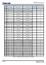
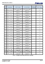
The other pin assignments for the high speed lanes are provided in the pinout attached to the
The PCI Express specification requires that all add-in cards be ready for enumeration within 120ms after power
is valid (100ms after power is valid + 20ms after PERST is released). The ADM-VPX3-9V2 does not meet this
requirement, but will configure in about 200ms when configured from a tandem bitstream with the proper SPI
constraints detailed in the llink:section:Configuration From Flash Memory. For more details on tandem
configuration, see Xilinx XAPP 1179.
Note:
Different SBCs/backplanes will benefit from different RX equalization schemes within the PCIe IP core
provided by Xilinx. Alpha Data recommends using the following setting if a user experiences link errors or
training issues with their system: within the IP core generator, change the mode to "Advanced" and open the
"GT Settings" tab, change the "form factor driven insertion loss adjustment" from "Add-in Card" to
"Chip-to-Chip" (See Xilinx PG195, PG213, and PG239 for more details).
Page 15
Functional Description
ad-ug-1377_v1_2.pdf


