background image

If you forget your V-Chip Password 

- Omnipotence V-Chip Password: 3308

- Press MENU button. 

- Press MENU buttons to highlight "CCD\V-CHIP" Menu. 

- Press Up, Down buttons to highlight "

鳐軐鷐槐

盐賐

釐鋐駐

". 

- Press Up, Down buttons to highlight "

賐釐諐韐

郐軐槐

駐諐鳐

鳐㑜飐鯐跐

". 

- Use the Number buttons (0~9) to enter an omnipotence Password. 

- Press MENU button to confirm and your can select "CHANGE PASSWORD". 

- Suggest: Change to your familiar Password again. 


Software upgrade 

- Connect the RS-232C input jack to an external control device (such as a 

computer) and software upgrade. 


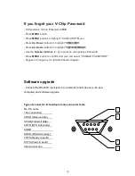
Type of connector; D-Sub 9-pin male connector male   

No. Pin name   

1 No connection                   

2 RXD (Receive data)         

3 TXD (Transmit data)       

4 DTR (DTE side ready)     

5 GND                                     

6 DSR (DCE side ready)     

7 RTS (Ready to send)       

8 CTS (Clear to send)         

9 No Connection                   


id39543029 pdfMachine by Broadgun Software  - a great PDF writer!  - a great PDF creator! - http://www.pdfmachine.com  http://www.broadgun.com 

30

Содержание LCT2016

Страница 1: ...cification 25 25 Mechanical Dimensions 26 26 Disassembly 27 28 Spare parts list 29 29 V chip password and software upgrade 30 32 Model SERVICE MANUAL This manual is the latest at the time of printing and does not include the modification which may be made after the printing by the constant improvement of product ...

Страница 2: ...ightness The high voltage must not exceed 30 KV under any circumstances Each time when a receiver requires servicing the high voltage should be checked The reading of the high voltage is recommended to be recorded as a part of the service record It is important to use an accurate and reliable high voltage meter 2 The only source of X RAY RADIATION in this TV receiver is the picture tube For contin...

Страница 3: ...orks etc 6 When servicing is required observe the original lead dressing Extra precaution should be given to assure correct lead dressing in the high voltage area 7 Keep wires away from high voltage or high tempera ture components 8 Before returning the set to the customer always perform an AC leakage current check on the exposed metallic parts of the cabinet such as antennas terminals screwheads ...

Страница 4: ...colors R G B each 256 scales Gray Scale 256 R G B each 8 bit Brightness Peak Value 450cd m2 Typical Contrast Dark Room 500 1 Typical TV System NTSC M Power Supply AC 100 240V 50 60 Hz Power Consumption 60W Input Terminals PC VGA 15 Pin Analog RGB Input Component Video YPbPr YCbCr x 1 RCA Terminals Video Input RCA Terminals S Video Input Mini Din 4 Pin Terminal Audio Input for Video S Video Audio I...

Страница 5: ...86 72 81 31 50 5 720 x 400 31 47 70 08 28 32 6 800 x 600 35 16 56 25 36 00 7 800 x 600 37 90 60 32 40 00 8 800 x 600 46 90 75 00 49 50 9 800 x 600 48 08 72 19 50 00 10 832 x 624 49 00 75 00 57 27 11 1024 x 768 48 40 60 00 65 00 12 1024 x 768 56 50 70 00 75 00 13 1024 x 768 60 00 75 00 78 75 14 1152 x 864 63 86 70 02 94 51 15 1152 x 864 67 52 75 02 108 03 16 1280 x 960 60 02 60 02 108 04 17 1280 x ...

Страница 6: ...ng off To cancel sleep time press SLEEP repeatedly until sleep OFF appears VOL Press to adjust the volume CH Press to scan through channels To scan quickly through channels press and hold down either channels MENU Press to enter into the on screen setup menu press again to exit Press to move the on screen cursor R P MODE Press repeatedly to cycle through the picture mode STANDARD BRIGHT MOVIE or U...

Страница 7: ...in Offset Color Space Conversion C Y Output Formatter Y 9 0 YCbCr VBI Data Slicer Copy Protection Detector C 9 0 Host Interface Timing Processor With Sync Detector VI_1_A VI_1_B VI_1_C VI_2_A VI_2_B VI_2_C VI_3_A VI_3_B VI_3_C VI_4_A CVBS Y G CVBS Pb B C CVBS Pr R C CVBS Y CVBS Y G Analog Front End Sampling Clock GPIO FSS HS CS VS VBLK FID AVID XTAL1 XTAL2 DATACLK RESETB GLCO PWDN SCL SDA YCbCr 6 ...

Страница 8: ... S 3 G 4 D 5 D 6 D 7 D 8 1U3 FDS9435 SOP08 1U3 FDS9435 SOP08 1R14 10K 1R14 10K 1C3 100nF 1C3 100nF 1C10 100nF 1C10 100nF 1C15 100nF 1C15 100nF 1C30 100nF NC 1C30 100nF NC 1R21 10K 1 1R21 10K 1 1R4 100 1R4 100 1C14 100nF 1C14 100nF 1R2 10K 0 1R2 10K 0 1L4 33uH SMT L 1 1L4 33uH SMT L 1 BS 1 IN 2 SW 3 GND 4 N C 8 EN 7 COMP 6 FB 5 1U4 MP1410 1U4 MP1410 1C19 100nF 1C19 100nF 1TVS 1805 1TVS 1805 1R6 10K...

Страница 9: ...10K 2RP2 10K 2R14 4K7 2R14 4K7 2EC3 47U 16V 2EC3 47U 16V 2C6 104 2C6 104 3 1 2 2Q1 PMBS3906 2Q1 PMBS3906 2R13 5 1K 2R13 5 1K 2R19 4K7 2R19 4K7 2D1 4148 2D1 4148 1 2 3 4 5 6 7 8 9 2CON1 HEADER 9 2CON1 HEADER 9 1 2 3 4 5 2CON2 HEADER 5 2CON2 HEADER 5 1 2 3 4 5 6 7 8 2RP1 10K 2RP1 10K 2R8 10K 2R8 10K A0 1 A1 2 A2 3 GND 4 SDA 5 SCL 6 WP 7 VCC 8 2U2 24C16 2U2 24C16 2R16 101 2R16 101 EA VP 35 XTAL1 21 X...

Страница 10: ...D 57 GND 59 GND 76 VDDC 19 VDDC 102 VDDC 114 VDDC 142 VDDP 10 VDDP 22 VDDP 88 VDDP 99 VDDP 111 VDDP 129 VDDP 139 AVDD_DVI 48 AVDD 54 AVDD 58 AVDD 77 BIN0M 69 BIN0 70 GIN0M 71 GIN0 72 SOGIN0 73 RIN0M 74 RIN0 75 H_SYNC0 38 V_SYNC0 39 DDC1_DAT 29 DDC1_CLK 30 REXT 55 RMID 78 REFM 80 REFP 79 CS 82 SDA 83 SCL 84 INT 85 DDCROM_CLK 31 DDCROM_DAT 32 PWM0 86 PWM1 87 XIN 34 XOUT 35 GND 101 BYPASS 2 VCLK 90 V...

Страница 11: ...00nF 4C59 100nF 4C59 100nF 4C53 100nF 4C53 100nF 4C43 NC 100nF 4C43 NC 100nF 4C25 100nF 4C25 100nF 4C51 330pF 4C51 330pF 4L3 FB 0805 4L3 FB 0805 4L6 2 7uH 0805 4L6 2 7uH 0805 4C24 330pF 4C24 330pF 4C7 100nF 4C7 100nF 4C6 100uF 16V 4C6 100uF 16V 4C37 33pF 4C37 33pF 4C3 100uF 16V 4C3 100uF 16V 4C16 100nF 4C16 100nF 4R5 33 4R5 33 1 2 3 4D2 BAV99 4D2 BAV99 4L13 2 7uH 0805 4L13 2 7uH 0805 4C20 100uF 16...

Страница 12: ...6V 5R25 6 8K 5R25 6 8K 5R7 100 5R7 100 5C14 100nF 5C14 100nF 5R22 75 330 5R22 75 330 5Y1 12MHz 5Y1 12MHz 5R1 100 5R1 100 5R24 470 5R24 470 5C12 100nF 5C12 100nF 5R4 12K 5R4 12K 5C1 104 5C1 104 5C2 100uF 16V 5C2 100uF 16V 5R12 4 7K 5R12 4 7K 5R2 100 5R2 100 5C16 100nF 5C16 100nF 5C11 100nF 5C11 100nF 5R3 100K 5R3 100K 5C19 100nF 5C19 100nF 5C10 150pF 5C10 150pF VDDA 31 P0 5 19 P0 4 18 P3 0 ADC0 9 P...

Страница 13: ...24 100nF 6C24 100nF 6C30 47pF NC 6C30 47pF NC 6C61 104 6C61 104 6BR2 FB 6BR2 FB 6C45 104 6C45 104 6R1 2 4K 6R1 2 4K 6C28 4 7uF 6C28 4 7uF 6C1 10uF 6C1 10uF 6C8 470nF 6C8 470nF 6R16 3 3K 6R16 3 3K 6C43 104 6C43 104 6C4 1uF 6C4 1uF 6FB7 50 0805 6FB7 50 0805 1 2 3 6CON5 S_VIDEO_L 6CON5 S_VIDEO_L 6C13 33nF 6C13 33nF 6C54 272 6C54 272 6C33 10uF 6C33 10uF 6R11 10K 6R11 10K 6R3 2 4K 6R3 2 4K 6C39 101P 6C...

Страница 14: ...N1 17 I2S_DA_IN2 21 I2S_CL 14 I2S_DA_OUT 16 DACM_L 27 DACM_R 26 SC1_OUT_L 31 SC1_OUT_R 30 D_CTR_I O_0 9 D_CTR_I O_1 8 TESTEN 4 VREFTOP 42 AGNDC 36 XTAL_IN 5 XTAL_OUT 6 CAPL_M 34 VREF1 29 VREF2 25 DVSS 20 AHVSS 35 AVSS 44 N C 28 N C 32 N C 24 N C 23 RESETQ 22 DVSUP 19 AHVSUP 33 AVSUP 1 TP 7 ADR_CL 18 7U2 MSP34x5G QFP44 6 7U2 MSP34x5G QFP44 6 7R8 100 7R8 100 7R5 100 7R5 100 1 2 3 7Q2 2N3904 NC 7Q2 2...

Страница 15: ...IGHT BBO 7 0 BAO 7 0 GAO 7 0 RAO 7 0 PANEL_VCC PANEL_VCC 5VCC 12VCC 5VCC PANEL_VCC PANEL_VCC 5VCC H_SYNCOUT V_SYNCOUT CLKO DENO H_SYNCOUT V_SYNCOUT DENO CLKO ADJ_BACKLIGHT PANEL_BACKLIGHT Title Size Document Number Rev Date Sheet of 1 0 A3 9 11 Title Size Document Number Rev Date Sheet of 1 0 A3 9 11 Title Size Document Number Rev Date Sheet of 1 0 A3 9 11 Backlight 1 2 3 4 5 6 7 8 4x33 NC 4x33 NC...

Страница 16: ...R15 101 9R16 75 9R16 75 9C6 473 9C6 473 1 2 3 9D3 BAV99 9D3 BAV99 9R6 101 9R6 101 1 2 3 9D2 BAV99 9D2 BAV99 9C30 473 9C30 473 9C17 104 9C17 104 9R13 101 9R13 101 9R3 101 9R3 101 9C26 NC 9C26 NC 9R20 101 9R20 101 9C29 473 9C29 473 9C28 NC 9C28 NC 9R22 1K 9R22 1K 5 6 9J1C 9J1C 9L7 FB 0805 9L7 FB 0805 9L4 FB 0805 9L4 FB 0805 9C22 NC 9C22 NC 9R8 75 9R8 75 9R10 101 9R10 101 9C31 473 9C31 473 9C9 NC 9C9...

Страница 17: ...100nF DGND 1 TESTIC1 2 TESTIC2 3 TESTO1 4 TESTO2 5 TESTO3 6 TESTO4 7 TESTO5 8 TESTO6 9 TESTO7 10 TESTO8 11 TESTO9 12 EXTALTF 13 EXTDYCO0 14 EXTDYCO1 15 EXTDYCO2 16 EXTDYCO3 17 EXTDYCO4 18 EXTDYCO5 19 EXTDYCO6 20 EXTDYCO7 21 EXTDYCO8 22 EXTDYCO9 23 DGNDRAM 24 DGNDRAM 25 DVDDRAM 26 DVDDRAM 27 TEST10 28 TEST11 29 TEST12 30 DVDDIO 31 TEST13 32 DGND 33 AGND 34 AGND 35 XI 36 XO 37 AVDD 38 DVDD 39 TEST14...

Страница 18: ...17 ...
Страница 19: ...CB170 0 1uF TP12 TP22 TP31 R361 33 R231 33 TP16 R215 100 R217 0 CE110 10uF 25v CB168 0 1uF R232 33 TP17 R241 0 CE63 10uF 25v R242 0 U28 WM8776 1 2 3 4 5 6 7 8 9 10 11 12 13 14 15 16 17 18 19 20 21 22 23 24 25 26 27 28 29 30 31 32 33 34 35 36 37 38 39 40 41 42 43 44 45 46 47 48 AIN2L AIN1R AIN1L DACBCLK DACMCLK DIN DACLRC ZFLAGR ZFLAGL ADCBCLK ADCMCLK DOUT ADCLRC DGND DVDD MODE CE DI CL HPOUTL HPGN...

Страница 20: ...DD SVM LVDS AP 0 7 3 AN 0 7 3 CLK1 3 CLK1 3 CLK2 3 CLK2 3 G 3 R 3 B 3 SVM 3 VSYNC 3 HSYNC 3 GPIO 3 VCC 12V L75 0 082uH L IND SMD 0603 R279 75 1 CB185 0 1uF L3 FB BEAD SMD 0805 C149 33pF CE87 220uF 16v C155 33pF R366 75 F1 4A v FUSE DIP P10 0 J9 8x1 W HOUSING DIP8 W H P2 54 1 2 3 4 5 6 7 8 CE86 330uF 25v C330UF25V D8H14 C154 33pF R281 75 1 J8 FI SE30P HF LVDS 30P P1 25 S 1 2 3 4 5 6 7 8 9 10 11 12 ...

Страница 21: ...ing UP3_0 PWM0 LED_GRN UP3_1 6 8 OBO0 3 OBO1 3 OBO2 3 OBO3 3 OBO4 3 OBO5 3 URST 3 6 IR 3 OBO6 3 OBO7 3 UP1_2 6 UP3_0 6 PWM0 3 DV33A 5VSB DV33A VCC VCC VCC 5VSB L89 FB BEAD SMD 1206 R4 510 R290 0 R291 10k L85 FB Q13 2N3904 SOT23 SMD 1 3 2 R14 10K R0603 SMD R ANGLE J10 12x1 W HOUSING R A DIP12 WH P2 0 R 1 2 3 4 5 6 7 8 9 10 11 12 R293 4 7k R285 10k R288 4 7k R57 0 CE2 470uF 50v L82 FB CB2 0 1uF R286...

Страница 22: ...1 2 1C6 10nF 1 2 CE7 33uF 16V 1 2 1R5 100 1 2 1L5 FB 2 2 3 3 4 4 5 5 9 9 8 8 7 7 6 6 NC 1 M1 GND HOLE 1 2 1L6 FB 1 2 CE8 100uF 16V 1 2 FB2 0 1 2 1R15 0 1 2 1R12 71 5 1 2 1R6 100 1 2 1C1 10nF 1 2 CE3 100uF 16V 1 2 CB6 0 1uF 1 2 3 4 5 6 7 8 9 10 11 12 1J1 CON12 1 2 1R9 0 1 2 1C8 820pF 560pF 1 2 CB3 0 1uF 1 2 CE9 220uF 16V 1 2 1C7 820pF 560pF 1 2 1R8 1k 1 2 CB7 0 1uF 1 2 1R10 220 1 2 1R3 56 1 2 CE4 1...

Страница 23: ...0K 5 1 2 L5 10uH 1 2 R37 10K 5 1 2 R12 10K 5 1 2 C10 100UF 25V 1 2 R17 100K 5 C41 22pF 1 2 C35 100NF X7R 1 2 R4 100K 5 1 2 C21 22pF NPO 1 2 C4 100UF 25V 1 2 R8 10 5 1 2 C16 100NF X7R 5 6 OUT 7 U2B RC4558 1 2 R22 10 5 1 2 R3 10K 5 1 2 C8 4 7nF NPO 1 2 R11 10K 5 C14 22UF 16V 1 2 C28 100NF X7R C19 22UF 16V D3 MBRS130LTR 1 2 C6 100NF X7R D2 6 2V 1 2 L6 10uH 1 2 R9 10K 5 1 2 R6 10 5 3 2 OUT 1 U2A RC455...

Страница 24: ...D9 1N4148 MUTEB AGND AGND D10 NC R43 0R AGND AGND LOUT ROUT AUSPL AUSPR 1 2 R57 4K7 5 1 2 R63 10K 5 1 2 R48 1k8 5 C2 100U 35V 1 2 R58 4K7 5 5 6 OUT 7 U5B RC4558 1 2 R52 22K 5 1 2 R49 4K7 5 1 2 R59 10K 5 1 2 C45 1n 1 2 R65 47K 5 1 2 R50 4K7 5 1 2 R54 10K 5 1 2 C46 1n 2 R60 5 3 2 OUT 1 U5A RC4558 1 C47 C43 10U 16V 1 2 R51 10K 5 1 2 R55 10K 5 2 R61 47K 5 1 C48 C44 22U 16V 1 2 C49 22P C22 22U 16V 1 2 ...

Страница 25: ...30K R51 120K R54 43K R52 1K D11 1N4148 Q6 BC327 SHORT CIRCUIT PROTECTION C52 22NF 1 2 3 4 5 6 7 8 J1 PH 2 0 1 2 3 4 5 J2 PH2 0 1 2 3 4 5 6 J3 PH2 5 1 2 3 4 J4 PH2 0 5V 5V 5V GND GND GND 12V 12V 5VS 5VS GND GND ON OFF 24V 24V 24V GND GND GND 24VA 24VA GND GND 0 45 0 28 1 2 5 6 13 3 8 9 10 14 4 12 TR3 Vstr 6 NC 5 Vfb 4 Vcc 3 Drain 1 GND 2 U5 FSDM0565 R67 10R R49 10R R70 1 2K R72 5 6K R71 5 6K R69 1 ...

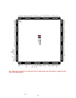
Страница 26: ...7 BA 6 GND AVDD_ADC GND AVDD_ADC 39 40 GND NC 80 79 78 77 76 75 74 73 72 71 70 69 68 67 66 65 AVDD_ADC REFP REFM 103 104 105 106 107 108 109 110 111 112 113 114 115 116 117 118 119 120 121 122 123 124 125 126 127 128 ECLK BB 0 BB 1 BB 2 BB 3 VDDP GND BB 4 129 130 131 132 133 134 135 136 137 138 139 140 141 142 143 144 145 146 147 148 149 150 151 152 153 154 155 156 157 158 159 160 NC NC HSYNC1 VSY...

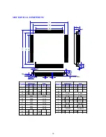
Страница 27: ... 0 098 0 107 0 114 D 31 20 1 228 D1 28 00 1 102 D2 25 35 0 998 E 31 20 1 228 E1 28 00 1 102 E2 25 35 0 998 R1 0 13 0 005 R2 0 13 0 30 0 005 0 012 Millimeter Inch Symbol Min Nom Max Min Nom Max θ 0 7 0 7 θ1 0 0 θ2 8 Ref 8 Ref θ3 8 Ref 8 Ref b 0 22 0 30 0 38 0 009 0 012 0 015 c 0 11 0 15 0 23 0 004 0 006 0 009 e 0 65 BSC 0 026 BSC L 0 73 0 88 1 03 0 029 0 035 0 041 L1 1 60 Ref 0 063 Ref S 0 20 0 008...

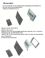
Страница 28: ...Removal of the Back Cover Disassembly 2 Removal of the MAIN PCB a Remove the screws b slide out the LCD chassis slightly pull up the connector of AC cord from PCB pull up the LCD PCB from LCD c Remove the A node cap from The picture tube To avaid a shock hazard be sure to discharge d Take out the LCD chassis 27 ...

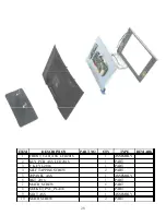
Страница 29: ...FRONT_CAB_ASS_LCD2016 1 ASSEMBLY 2 KEY_PCB_ASS_LCD2016 1 PART 3 F_KEY_L2016 1 PART 4 SELF TAPPING SCREW 2 PART 5 20PANEL_ASS 1 ASSEMBLY 6 BKT_2016 1 PART 7 MACH_SCREW 6 PART 8 SOCKET_PVC_PLATE 1 PART 9 SEAT_ASS 1 ASSEMBLY 10 MACH SCREW 2 PART 28 ...

Страница 30: ...verter PCBA 1 piece 8 TI L20160008 01 Control PCBA with 8 pin connector 1 piece 9 TI L20160009 01 AC Adaptor with AC Cord 1 piece 10 TI L20160010 01 5 pin connector 1 piece 11 TI L20160011 01 6 pin connector 1 piece 12 TI L20160012 01 LVDB signal cable 1 piece 13 TI L20160013 01 Remote Control 1 piece 14 TI L20160014 01 Speaker 2 piece 15 TI L20160015 01 Model Plate 1 piece 16 TI L20160016 01 Poly...

Страница 31: ...r an omnipotence Password Press MENU button to confirm and your can select CHANGE PASSWORD Suggest Change to your familiar Password again Software upgrade Connect the RS 232C input jack to an external control device such as a computer and software upgrade Type of connector D Sub 9 pin male connector male No Pin name 1 No connection 2 RXD Receive data 3 TXD Transmit data 4 DTR DTE side ready 5 GND ...

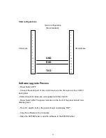
Страница 32: ...on the LCD TV back panel VGA connection cables are not supplied with the LCD TV Power Switch ON The power indicator on the front of the panel should now display green Press V and V button the panel should now display ISP Copy the software to the computer Open the 8051ISPwriter Load the software to the 8051ISPwriter 1 2 3 4 5 6 7 8 9 10 11 12 13 14 15 1 2 3 4 5 6 7 8 9 10 11 12 13 14 15 31 ...

Страница 33: ...which will be update Press ConNect button Waiting for the upgrader programing when it is finished the bar will display program OK After the upgrader is finished shut down the power switch take out the VGA connection 32 ...

Отзывы: