background image

DISASSEMBLY INSTRUCTIONS

B2-2

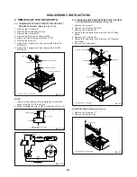
2-6:

2-4:

Remove the screw (1).
Remove the Disc L Lever and Disc L Lever Spring.
Remove the Stopper Spring.
Unlock the support (2) and remove the Locker Stopper.
Unlock the support (3) and remove the Disc Stopper.
Remove the Upper Roller, Roller Rubber and Roller
Gear.

1.
2.
3.
4.
5.
6.

DISC L LEVER/DISC STOPPER/LOCKER STOPPER/
ROLLER GEAR (Refer to Fig. 2-4-A)

Fig. 2-4-A

Disc L Lever

(1)

Disc L Lever Spring

Stopper Spring

Locker Stopper

(2)

(3)

Disc Stopper

Upper Roller

Roller Rubber

Roller Gear

• Screw Torque: 1.1 ± 0.2kgf•cm

2-5:

Remove the Guide Arm Spring.
Unlock the 3 supports (1) and remove the Rack Loading.
Remove the Rack Gear and Mid Rack Gear.

1.
2.
3.

Fig. 2-5

RACK LOADING/RACK GEAR/GUIDE ARM
SPRING/MID RACK GEAR (Refer to Fig. 2-5)

NOTE

1. In case of the Upper Roller installation, install correctly

as Fig. 2-4-B.

Fig. 2-4-B

[OK]

[NG]

Upper Roller

Upper Roller

Roller Gear

Roller Gear

Rack Loading

Guide Arm Spring

Rack Gear

Mid Rack Gear

LINK R ASS'Y/LINK L/LINK MID/LINK SPRING
(Refer to Fig. 2-6)

Remove the screw (1).
Remove the Link Spring.
Unlock the support (2) and remove the Link L.
Unlock the support (3) and remove the Link Mid.
Remove the screw (4).
Unlock the 4 supports (5) and remove the Link R Ass'y.

1.
2.
3.
4.
5.
6.

Fig. 2-6

• Screw Torque: 0.7 ± 0.1kgf•cm (Screw 

(1)

)

• Screw Torque: 1.5 ± 0.2kgf•cm (Screw 

(4)

)

(1)

Link Spring

Link L

(2)

(3)

Link Mid

(4)

Link R Ass'y

(5)

(5)

(5)

(5)

(1)

Mid Roller Gear 2

Arm Roller Ass'y

Terminal Gear

Mid Roller Gear 1

Fig. 2-7

• Screw Torque: 1.5 ± 0.2kgf•cm

2-7: ARM ROLLER ASS'Y/MID ROLLER 1/2 GEAR/

TERMINAL GEAR (Refer to Fig. 2-7)

Remove the screw (1).
Remove the Arm Roller Ass'y.
Remove the Terminal Gear and Mid Roller Gear 1.
Unlock the support (2) and remove the Mid Roller Gear 2.

1.
2.
3.
4.

(2)

(1)

(1)

(1)

Содержание CFTD2052

Страница 1: ...SERVICE MANUAL CFTD2052 Design and specifications are subject to change without notice ORIGINAL MFR S VERSION A LCD COLOR TELEVISION DVD VIDEO PLAYER...

Страница 2: ...IES WITH FDA RADIATION PERFORMANCE STANDARDS 21 CFR SUBCHAPTER J Location of the required Marking The rating sheet and the safety caution are on the rear of the unit PREPARATION OF SERVICING The laser...

Страница 3: ...nal on TV and turn on the TV Insulation resistance between the cord plug terminals and the eternal exposure metal Note 2 should be more than 1M ohm by using the 500V insulation resistance meter Note 1...

Страница 4: ...al power company For units intended to operate from battery power or other sources refer to the operating instructions GROUNDING OR POLARIZATION This unit is equipped with a polarized alternating curr...

Страница 5: ...equipment turn off the power and unplug all of the equipment from the wall outlet Failure to do so may cause an electric shock and serious personal injury Read the owner s manual of the other equipme...

Страница 6: ...CAL CODE ANTENNA DISCHARGE UNIT NEC SECTION 810 20 ANTENNA LEAD IN WIRE GROUNDING CONDUCTORS NEC SECTION 810 21 GROUND CLAMPS POWER SERVICE GROUNDING ELECTRODE SYSTEM NEC ART 250 PART H GROUND CLAMP E...

Страница 7: ...DVD Deck Rack Loading PARENTAL CONTROL RATING LEVEL 4 DIGIT PASSWORD CANCELLATION If the stored 4 digit password in the Rating Level menu needs to be cancelled please follow the steps below Turn Unit...

Страница 8: ...AMS MPEG MICON DSP MEMORY2 RF AMP AUDIO VIDEO MOTOR DRIVE REGULATOR2 OPERATION2 TUNER STEREO MICON SOUND AMP IN OUT POWER OPERATION AV JACK REMOCON DECODER SCALER1 SCALER2 LVDS TV POWER INVERTER START...

Страница 9: ...times CD Slow speed Fwd 1 7 1 2 times Actual Rev 1 7 1 2 times Actual G 3 Tuning Broadcasting System US System M System Tuner and System 1Tuner Receive CH Destination US W CABLE Tuning System F Synth...

Страница 10: ...Sound System No AV2 Output Source No Control Level Yes Volume Yes Brightness Yes Contrast Yes Color Yes Tint Yes Sharpness Yes Bass Yes Treble Yes Balance Yes Stereo Yes Pin Code No CH AV DVD Yes Com...

Страница 11: ...Yes Marker No Yes Program Play Back Yes CD MP3 Surround On Off No Screen Saver No MP3 Folder Name Yes File Name Yes File No Yes Time Yes Track No Yes G 11 OSD Language TV English French Spanish DVD En...

Страница 12: ...t A B Yes Zoom Quick View Yes Mute Yes Sleep Yes Jump Closed Caption Yes Freeze frame Yes G 14 Features CATV Yes Auto Shut Off Yes Auto CH Memory Yes V Chip Yes Type USA Type Auto Search No SAP Yes PC...

Страница 13: ...in No Registration Card No Information Sheet Yes 75 ohm Coaxial Cable w Core Yes 300 ohm to 75 ohm Antenna Adapter No G 16 Interface Switch Front Power Tact Yes Channel Up Yes Channel Down Yes Volume...

Страница 14: ...t Box Yes Material Double White W Color Photo Label No W Handle No Dimensions W x D x H mm 694x535x295 Design As Per Buyer s Description of Origin Yes Drop Test 1 Corner 3 Edges 6 Surfaces Height cm 6...

Страница 15: ...screw 2 Remove the 4 screws 3 Remove the 2 screws 4 Remove the Jack Plate and Jack Shield in the direction of arrow B Remove the 3 screws 5 Remove the Back Angle in the direction of arrow C Fig 1 4 1...

Страница 16: ...emove the Operation 2 PCB in the direction of arrow B Fig 1 6 Side Panel 1 1 A B Operation 2 PCB 2 2 2 NOTE Use the Lead Free solder and the exclusive soldering iron Manual soldering conditions Solder...

Страница 17: ...he following connector CP3802 Remove the 4 screws 1 Remove the Power PCB in the direction of arrow Fig 1 10 1 1 1 1 Power PCB 1 9 BACK LIGHT PCB Refer to Fig 1 9 1 2 3 Disconnect the following connect...

Страница 18: ...et 1 1 1 1 1 1 1 2 2 2 1 13 1 2 3 4 Remove the 2 screws 1 Remove the Operation 1 PCB in the direction of arrow A Remove the 2 screws 2 Remove the Remocon PCB in the direction of arrow B 2 OPERATION 1...

Страница 19: ...1 1 Motor Loading Worm Start SW PCB Ass y 2 2 3 4 4 5 5 End SW PCB Ass y 29 7 0 1mm Safety surface for pressing of the insert Motor Loading Worm Fig 2 1 C Start SW PCB Ass y End SW PCB Ass y Motor Red...

Страница 20: ...1 In case of the Upper Roller installation install correctly as Fig 2 4 B Fig 2 4 B OK NG Upper Roller Upper Roller Roller Gear Roller Gear Rack Loading Guide Arm Spring Rack Gear Mid Rack Gear LINK R...

Страница 21: ...8 A Unlock the support 1 and remove the Clamper Ass y Unlock the support 2 and remove the Disc Guide Arm Unlock the support 3 and remove the Disc R Lever 1 2 3 Clamper Ass y 1 3 2 Disc Guide Arm Disc...

Страница 22: ...the IC leads using a blower type IC desoldering machine Refer to Fig 3 2 2 Fig 3 2 NOTE Do not rotate or move the ic back and forth until IC can move back and forth easily after desoldering the leads...

Страница 23: ...8 Thin tip Soldering Iron NOTE When the IC leads are bent during soldering and or repairing do not repair the bending of leads If the bending of leads are repaired the pattern may be damaged So alway...

Страница 24: ...r more than the standard time in the appropriate condition See below chart Releasing of V CHIP PASSWORD Initialization of factory data on TV NOTE If you set factory initialization the memories are res...

Страница 25: ...the remote step through the ADDRESS until required ADDRESS to be changed is reached Press ENTER to select DATA When DATA is selected it will blink Again step through the DATA using VOL UP DOWN button...

Страница 26: ...wire be sure to put the wire back in its original position When you exchange IC and Transistor with a heat sink apply silicon grease on the contact section of the heat sink Before applying new silicon...

Страница 27: ...THON C DRREF C RCUT2 C GCUT2 C BCUT2 C GAINR C GAING C GAINB C RCUT W GCUT W BCUT W DRI1 W DRI2 W MD6 W DTHON W DRREF W RCUT2 W GCUT2 W BCUT2 W GAINR W GAING W GAINB W BRI CEN BRI MAX BRI MIN CON CEN...

Страница 28: ...ER LCD PANEL S3602 S3601 CD3601 AC IN POWER PCB CD503 CD501 CD701 CP2301 CP2302 CP2601 CD2301 CD2302 CD2601 DVD PCB CP7005 CP7006 CP7001 CP7002 CP7003 CD7001 CP7004 BACK LIGHT PCB CD705 J1001 J792 J79...

Страница 29: ...DATA SCLK FNN FNP VBIASS0 S1 D D D E MD MC ML AMCLK ABCLK ASDATAO ALRCLK B U AUDIO R DVD RESET Y V AUDIO L TV BLOCK ZERO TR FO DISC_IN DISC_END SW TX SPDIF RX A P CON 7V_D B P CON 5V_D C P CON A5V_D D...

Страница 30: ...TROLLER IC7002 TH12A TV BLOCK DIAGRAM FROM DVD PCB DVD_Y DVD_U DVD_V USA STEREO IC901 AN5832SA E1V SW IC905 IC906 NJM2534V TE2 SW IC903 IC904 MM1501XNRE L R AV2 L R SPIF 134 COAXIAL J701 V V VIDEO_OUT...

Страница 31: ...05 PQ070XZ01ZPH P CON 32V P CON 3 3V P CON 3 3V P CON 1 5V SOUND B INVERTER P CON 9V E 5 E 6 POWER BLOCK DIAGRAM P CON 2 5V Q3001 F3001 ADAPTER 12V GND DVD POWER H 2CH SW REG CONTROLLER IC3001 BA9743A...

Страница 32: ...E 7 E 8 TRANSFORMER SWITCHING T3601 15 7 AC IN 9 CONTROL IC IC3603 ICE1QS01 D3603 3 7 4 F3601 Q3601 SWITCHING CD503 IC3602 PS2561AL1 1 V W 18 13 12 4 GND 13V 1 2 3 14V FEED BACK 16 1 2 3 1 2 3 D3606 D...

Страница 33: ...C676 PRINTED CIRCUIT BOARDS LCD TOP SIDE L821 C895 C634 C629 C887 C883 L819 C626 C621 C813 C654 C891 R858 C625 C658 C899 C824 C652 C631 C640 L603 C637 C894 C624 C888 C643 C890 C827 C829 R832 R859 C63...

Страница 34: ...7_1 R4046 R4049 R4050 R4051 C4002 C4003 C4090 C4089 C4088 C4004 C4038 CP2251 SW2253 SW2252 SW2254 SW2255 SW2251 C4007 R2601 R2610 R2315 C2333_1 C2334_1 C2329_1 HS2301 R4033 R4034 W813 C2608 R4052 R400...

Страница 35: ...1 C1047 C1034 C1027 C1043 C1028 D1001 L905 W022 C946 C954 W023 R1027 W048 W040 W041 W042 W051 W037 W049 W094 W107 W017 W108 W078 W080 W052 W818 W083 W046 W032 W064 W035 W038 W005 W011 W013 W014 W026 W...

Страница 36: ...710 R727 Q703 R749 C729 R717 C728 C752 R716 R715 R718 R719 R726 R724 R725 C757 R722 C730 R721 C721 C709 C742 C941 C953 C766 C764 R701 R702 C717 C716 R704 R707 R706 R703 Q702 Q701 R708 R764 R705 R765 C...

Страница 37: ...7093 CP7005 CP7006 CP7001 CP7002 CP7003 T7013 T7015 T7014 T7012 T7011 T7006 T7005 T7008 T7007 T7002 T7001 T7003 T7004 T7009 T7010 F7001 C7001 C7002 C7003 C7004 CD 700 1 IC7002 Q7016 Q7018 Q7017 Q7015...

Страница 38: ...HD6 HA19 SPINDLE_PWM HA20 HA8 SLED_PWM HD0 HD13 RESET SPD_FG HD1 HD5 HD2 TOUT_SW DISC_IN_SW HA20 HOME HOME HD3 HOME HD4 LDON SBMUTE HD5 HD12 PSMUTE HD6 WR DJTDO ML HD7 DISC_END_SW HD4 DJTDI MC HD8 HD9...

Страница 39: ...S RAMCAS SD_D10 SD_D5 SD_BA0 HD12 HA20 RAMDQM SD_D9 SD_D6 RAMWE RAMCLK HD4 WR HA0 SD_D8 SD_D7 HA1 RESET HA2 HA3 HA4 HD11 RAMDQM HA5 HA6 RAMDQM RAMWE HA7 HD3 HA8 RAMCLK RAMCAS HA9 HA10 HD10 HA19 RAMRAS...

Страница 40: ...8M R2633 4 7K R2626 390 R2631 2 2K R2638 2 2K R2632 100 R2637 1K B2601 FCM2012H 102T04 B2602 FCM2012H 102T04 B2605 FCM2012H 102T04 B2603 FCM2012H 102T04 B2604 FCM2012H 102T04 OF PRINTING AND SUBJECT T...

Страница 41: ...E LATEST AT THE TIME DURING PLAYBACK MEASURED WITH THE DIGITAL TESTER NOTE THE DC VOLTAGE EACH PART WAS DIGITAL AUDIO SIGNAL PB DAC_C U C_VIDEO DAC_B V Y_VIDEO DAC_A Y _VIDEO DAC_VIDEO_C DAC_VIDEO_B D...

Страница 42: ...1 B2301 FCM2012H 102T04 OF PRINTING AND SUBJECT TO CHANGE WITHOUT NOTICE NOTE THIS SCHEMATIC DIAGRAM IS THE LATEST AT THE TIME DURING PLAYBACK MEASURED WITH THE DIGITAL TESTER NOTE THE DC VOLTAGE EAC...

Страница 43: ...220 1 R3019 1 8K 1 R3018 8 2K 1 R3027 510 1 R3026 1 8K 1 R3013 560 R3029 1K 1 R3005 10K 1 R3015 10 R3020 560 R3022 10 R3021 5 6K R3012 56K R3003 1K R3002 5 6K R3001 10K R3006 68K R3004 10K 1 B3001 FCM...

Страница 44: ...ASURED CP2251 A2001WR2 2P 1 2 SW2255 EVQ21505R SKIP SW2254 EVQ21505R SKIP SW2251 EVQ21505R EJECT SW2252 EVQ21505R STOP SW2253 EVQ21505R PLAY R2251 820 R2252 1K R2253 1 5K R2254 2 7K R2255 6 8K OF PRIN...

Страница 45: ...KA C946 100 16V YK C905 2 2 50V KA C901 2 2 50V KA C913 2 2 50V KA C954 100 16V YK R002 100 R001 100 R901 180K R906 100 R902 3 3K R903 1 2K R904 1 2K R911 100 OF PRINTING AND SUBJECT TO CHANGE WITHOUT...

Страница 46: ...03 10K R113 4 7K R109 4 7K R161 4 7K R164 4 7K R117 4 7K R153 330 R123 10K R105 4 7K R135 3 3K R140 1K R144 1K R141 1K R104 10K 1 4W B101 HCB2012K 600T25 OF PRINTING AND SUBJECT TO CHANGE WITHOUT NOTI...

Страница 47: ...47 16V KA C1037_1 22 16V KA C1036 2 2 50V KA C1002 2 2 50V KA C1003 2 2 50V KA C1019 10 25V KA C1011 10 25V KA C1034 22 16V KA C1021 10 25V KA C1020 10 25V KA C1025 100 16V YK C1023 10 25V KA C1030 1...

Страница 48: ...04 220K R706 180K R721 10K R722 10K R726 12K R725 10K R724 2 7K R715 100K R716 10K R717 10K R723 470 R729 10K R744 470 R719 47K R720 100K 1 4W R718 47K R748 12K R764 47 R765 47 R709 100 1 2W R755 330...

Страница 49: ...2 B C3826 0 22 B C3802 0 1 B C3806 0 1 B C3808 0 022 B C3818 0 01 B C3811 0 0022 B C3821 0 1 B C3817 470P CH C3804 0 1 B C3807 27P CH C3829 0 01 B C3810_1 1000 16V YK C3815 100 25V YK C3816 100 16V YK...

Страница 50: ...505R POWER ON OFF SW2202 EVQ21505R VOL DOWN SINCE THESE PARTS MARKED BY CAUTION DESCRIBED IN PARTS LIST ONLY CRITICAL FOR SAFETY USE ONES ARE DANS LA NOMENCLATURE DES PIECES N UTILISER QUE CELLS DECRI...

Страница 51: ...V S C656 220 4V V S C609 330 4V V S C601 0 47 50V V S C604 0 47 50V V S C801 330 4V V S C877 330 4V V S R606 1 5K R623 1K R603 1 5K R618 470 R624 1K R604 1 5K R602 1 5K R601 1 5K R815 220 1 R817 1K 1...

Страница 52: ...6 NC_K5 NC_M3 NC_M5 NC_U4 NC_T1 NC_R3 NC_AA2 NC_AA3 NC_AA4 NC_AA25 NC_AB2 NC_AB3 NC_AB4 NC_AB23 NC_AB24 NC_AC3 NC_AC4 NC_AC5 NC_AC6 NC_AC7 NC_AC8 NC_AC10 NC_AC12 NC_AC16 NC_AC18 NC_V3 NC_V4 NC_V1 NC_W...

Страница 53: ...5V GND P CON 1 5V D_3 3V GND P CON 2 5V SCALER_V_OUT SDA SCL GND G 32 G 31 4 5 DRAM VDD 5 5 SCALER VDD LCD PCB SCALER2 SCHEMATIC DIAGRAM PCB340 TEDB66 TST2_IN 0 TST2_IN 1 TST2_IN 3 TST2_IN 2 TST2_IN...

Страница 54: ...WAS D EN_2 DCLK D EN_2 DCLK DRE7_2 DRE6_2 DRE5_2 DRE7_2 DRE4_2 DRE3_2 DRE6_2 DRE2_2 DRE5_2 DRE1_2 DRE0_2 DRE4_2 DGE7_2 DGE6_2 DRE3_2 DGE5_2 DGE4_2 DRE2_2 DGE3_2 DRE1_2 DGE2_2 DGE1_2 DRE0_2 DGE0_2 DBE...

Страница 55: ...ONTINUED PROTECTION AGAINST FIRE HAZARD POUR UNE PROTECTION CONTINUE LES RISQUES D INCEIE ATTENTION HS3603 763WAA0264 HS26V HS3601 763WAA0264 HS7V1 W805 W802 S D G Q3601 2SK3568 ORION_Q SWITCHING Q360...

Страница 56: ...R7066 680K 1 10W R7060 680K 1 10W R7054 680K 1 10W R7048 680K 1 10W R7042 680K 1 10W R7036 680K 1 10W R7118 680K 1 10W R7122 680K 1 10W R7094 680K 1 10W R7088 680K 1 10W R7082 680K 1 10W R7076 680K 1...

Страница 57: ...OUT NOTICE NOTE THIS SCHEMATIC DIAGRAM IS THE LATEST AT THE TIME DURING PLAYBACK MEASURED WITH THE DIGITAL TESTER NOTE THE DC VOLTAGE EACH PART WAS STEPPING_MOTOR B STEPPING_MOTOR B STEPPING_MOTOR A S...

Страница 58: ...U V V W W GND U V W INSW LOADING MOTOR SLED MOTOR SPINDLE MOTOR OPTICAL PICK UP PD LD DVD GND NC T DRV T RTN F DRV F RTN SLOT IN DVD DRIVE SW2 L H SW1 DVD CD GND VCC C B E F A Vref D VR COM VR CD GND...

Страница 59: ...the schematic diagram NOTE 1 3 2 6 7 10 9 MPEG MICON DSP AUDIO VIDEO 4 200ns 200mV 10ns 1 0V 200 s 500mV 200ns 500mV 500 s 500mV 500 s 500mV 10 s 100mV 10 s 100mV MEMORY2 RF AMP 5 200ns 200mV 8 10 s...

Страница 60: ...e corresponding balloon number in the schematic diagram NOTE 16 2ms 200mV 17 18 21 50ns 1 0V 22 0 5ms 1 0V 23 50 s 1 0V 25 20 s 1 0V 26 50 s 1 0V 27 10 s 1 0V MICON 19 20 10 s 0 5V 24 5ms 1 0V 28 10 s...

Страница 61: ...e point of the corresponding balloon number in the schematic diagram NOTE 31 32 1ms 200mV 33 34 2ms 0 5V IN OUT 2ms 50mV 1ms 200mV 35 2ms 0 5V 36 0 1 s 100mV 37 10 s 0 5V 38 10 s 0 5V DECODER 39 40 50...

Страница 62: ...209 209 102A 102C 201 102 201 201 127 123 125 102D 102B 202 102E 201 201 201 201 130 201 201 207 201 201 204 201 201 201 104A 104B 104B 104 104B 104B 104B 138 PCB280 OPERATION 2 PCB ASS Y 201 201 101...

Страница 63: ...4 113 106 124 203 204 124 204 124 114 206 204 124 124 PCB240 POWER PCB ASS Y PCBD20 AV PCB ASS Y PCB130 DVD PCB ASS Y 108 204 204 204 PCB340 LCD PCB ASS Y 204 107 204 204 111 204 111 135 204 204 204 2...

Страница 64: ...617 DVD DECK EXPLODED VIEW TOP VIEW I2 1 AB AB AB AB Applying positions AA and AB for the grease are displayed for this section Check if the correct grease is applied for each p osition NOTE CLASS MAR...

Страница 65: ...1 DK1 701 701 PCB590 END SW PCB ASS Y SW4 702 Applying positions AA and AB for the grease are displayed for this section Check if the correct grease is applied for each p osition NOTE CLASS MARK GREAS...

Страница 66: ...WCDA028 PAD 530x278 104A 704WPB0001 STAND 795WCDA029 PAD 350x278 104B 800WFA0061 CUSHION LEG A5N106A975 INSTRUCTION BOOK KIT J5N10602A WARRANTY SHEET 105 7A7050002A HANDLE ASS Y J5N10621A INSTRUCTION...

Страница 67: ...STOPPER DISC 621 92P200011A RUBBER ROLLER 622 92P300010A SPRING GUIDE ARM 623 92P300011A SPRING LEVER DISC L 624 92P300012A SPRING LINK 625 92P300013A SPRING STOPPER 626 92P000006A BRACKET LOADING MO...

Страница 68: ...KY SBR100 10J CBC11 Q101 TCAA3875SY TRANSISTOR SILICON KTC3875S_Y_RTK D3611 D28T0ERB20 DIODE RECTIFIER 10ERB20 TA1B2 Q105 TCAA3875SY TRANSISTOR SILICON KTC3875S_Y_RTK D3612 D28T0ERB20 DIODE RECTIFIER...

Страница 69: ...7 TCAA3875SY TRANSISTOR SILICON KTC3875S_Y_RTK J708 060G421034 RCA JACK HTJ 032 05AG COILS TRANSFORMERS J790 060J421036 RCA JACK MTJ 032 05A 30 FE L001 021673101J COIL 100 UH J791 060J421037 RCA JACK...

Страница 70: ...ONNECTOR PCB SIDE A2001WV2 2P CP701 069S2G0629 CONNECTOR PCB SIDE A2001WV2 16P CP703 069S240629 CONNECTOR PCB SIDE A2001WV2 4P CP705 069S280629 CONNECTOR PCB SIDE A2001WV2 8P CP802 06AEY05011 CONNECTO...

Страница 71: ...M5N1 06A O R NO SPEC NO W555001...

Отзывы: