background image

-35-

ELECTRICAL ADJUSTMENT-13/13

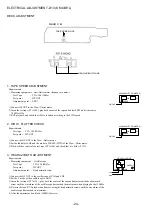
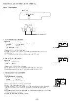
3. JITTER CHECK

1) While oscilloscope is kept connected in the same test point as in step2. RF

WAVEFORM CHECK, connect the output terminal of an oscilloscope to the
input terminal of the jitter meter.

2) Set the VOLT range selector of oscilloscope to 500mV range or below.
3) Play back 2nd track of TCD-782.
4) Check that jitter meter indicates 28.0ns or less.

4. PLAY ABILITY CHECK

1) Play back the 3rd , 8th and 13th track of ATD-001. Check that the noise does not

occur sound skipping does not occur.

5. LASER CURRENT CHECK

* Do not perform this measurement unless the laser is suspected to be defective.
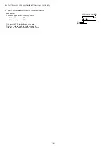
1) Connect digital multi-meter across the resistor R402(10

).

2) Play back the TCD-782 and check the DC voltage value on the digital multi-

meter.

3) Calculate the laser current (Iop) by dividing the DC voltage across R402 by the

resistor value (R402= 10

Ω)

. Check that the laser current (Iop) is 60mA or less.

OUTPUT

ns

OSCILLOSCOPE

JITTER METER

INPUT

RF SW

Vref

V

DIGITAL MULTIMETER

R402

R402

Содержание XR-M161HS(S)

Страница 1: ...CHANISM 2ZM 1 YR12NC BASIC CD MECHANISM DA11T3C XR M161HS BASIC CD MECHANISM KSM213CDM XR M161K COMPACT DISC STEREO SYSTEM XR M161 S M Code No 09 014 355 2N2 HS S K S SYSTEM XR M161HS S XR M161K S CD CASSEIVER CX SLM161 SPEAKER SX SLM161 ...

Страница 2: ... HS MODEL 21 SCHEMATIC DIAGRAM 5 5 CD K MODEL 21a FL ZCL 8 GRID ASSIGNMENT ANODE CONNECTION 1 1 22 ELECTRICAL ADJUSTMENT 23 35 CD TEST MODE 36 IC BLOCK DIAGRAM 1 2 37 IC BLOCK DIAGRAM 2 2 38 IC DISCRIPTION 1 3 LA9241ML 39 40 IC DISCRIPTION 2 3 LC78622NE 41 42 IC DISCRIPTION 3 3 LC867248A 5V96 43 44 MECHANICAL EXPLODED VIEW 1 1 45 MECHANICAL PARTS LIST 1 1 46 47 TAPE MECHANISM EXPLODED VIEW 1 1 2ZM...

Страница 3: ... 3 SPECIFICATIONS Design and specifications are subject to change without notice K MODEL HS MODEL Design and specifications are subject to change without notice ...

Страница 4: ...IB HS K B 161HSSC 1 8B CLB 905 110 IB K E B 161KSC 2 8A CLB 961 110 RC UNIT RC AAT11 3 87 A90 030 010 ANT LOOP AM NC C 4 87 043 115 010 ANT FEEDER FM 161HSSC 5 87 A90 118 010 ANT WIRE FM Z 161KSC 6 87 099 726 010 PLUG ADPTR CONV K 161KSC 7 87 A91 017 010 PLUG CONVERSION JT 0476 161HSSC ...

Страница 5: ...han those specified herein may result in hazardous radiation exposure ATTENTION L utilisation de commandes réglages ou procédures autres que ceux spécifiés peut entraîner une dangereuse exposition aux radiations ADVARSEL Usynlig laserståling ved åbning når sikkerhedsafbrydereer ude af funktion Undgå udsættelse for stråling This Compact Disc player is classified as a CLASS 1 LASER product The CLASS...

Страница 6: ...nnection remove solder shown in the right figure Body or clothes electrostatic potential could ruin laser diode in the optical block Be sure ground body and workbench and use care the clothes do not touch the diode Solder PICK UP Assy PWB SF P101NR PICK UP Assy PWB KSS 213C ...

Страница 7: ...E C120 87 010 545 080 CAP E 0 22 50 M 11L SME C121 87 010 401 080 CAP E 1 50 M 11L SME C122 87 010 401 080 CAP E 1 50 M 11L SME C125 87 010 401 080 CAP E 1 50 M 11L SME C126 87 010 401 080 CAP E 1 50 M 11L SME C129 87 A10 831 090 Elect Cap 1000uF 20 25V C130 87 A10 831 090 Elect Cap 1000uF 20 25V C131 87 A12 310 080 C CAP U 0 01UF 50V K X7R C132 87 A12 310 080 C CAP U 0 01UF 50V K X7R C133 87 A12 ...

Страница 8: ...200P 50 K B GRM C790 87 012 275 080 C CAP U 1200P 50 K B GRM C791 87 010 405 080 CAP E 10 50 M 11L SME C793 87 012 273 080 C CAP U 820P 50 K B C794 87 010 406 080 CAP E 22 50 M 11L SME C795 87 010 596 080 CAP S 0 047 16 C796 87 010 403 080 CAP E 3 3 50 M 11L SME C797 87 012 276 080 C CAP U 1500P 50 K B C798 87 012 276 080 C CAP U 1500P 50 K B C799 87 010 596 080 CAP S 0 047 16 C812 87 A12 310 080 ...

Страница 9: ...C CAP S 0 022 50 Z F C2012 C338 87 012 140 080 C CAP S 470P 50 J CH C339 87 010 405 080 CAP E 10 50 M 11L SME C340 87 010 405 080 CAP E 10 50 M 11L SME C341 87 010 318 080 C CAP S 47P 50 J CH GRM C342 87 010 318 080 C CAP S 47P 50 J CH GRM C345 87 012 272 080 C CAP U 680P 50V K X7R C346 87 012 272 080 C CAP U 680P 50V K X7R C350 87 010 374 080 CAP E 47 10 M 11L SME C351 87 010 234 040 Cap 47UF M E...

Страница 10: ...COG C214 87 010 314 080 C CAP S 22P 50V C215 87 012 176 080 C CAP U 15P 50 J CH C216 87 010 400 080 CAP E 0 47 50 M 11L SME C217 87 010 196 080 C CAP S 0 1 25 Z F C2012 C218 87 010 405 080 CAP E 10 50 M 11L SME CN201 87 099 720 010 CONN 30P BLK TYK B P CN202 87 A60 404 010 CONN 3P TKX P03P F1 FB201 87 A90 562 010 F BCAD 843556 TB36 TAPING 52mm L201 87 005 676 080 COIL 2 2UH K LF5 0S L202 87 A50 08...

Страница 11: ...C501 87 010 196 080 C CAP S 0 1 25 Z F C2012 C502 87 010 322 080 C CAP S 100P 50 J CH GRM C503 87 010 322 080 C CAP S 100P 50 J CH GRM C504 87 010 322 080 C CAP S 100P 50 J CH GRM C505 87 010 322 080 C CAP S 100P 50 J CH GRM C506 87 010 322 080 C CAP S 100P 50 J CH GRM C510 87 012 368 080 C CAP S 0 1UF 50V K X7R CN401 87 A60 424 010 CONN 16P V TOC B CN402 87 A60 670 010 CONN 6P H 2MM JMT CN403 87 ...

Страница 12: ... 6 0 8 0 45 2 1 25 0 45 3 2 1 6 108 118 128 A A CHIP RESISTOR PART CODE 0 55 Resistor Code Dimensions mm Symbol 1 16W 1005 5 CJ 1 0 0 5 0 35 104 L t W Regarding connectors they are not stocked as they are not the initial order items The connectors are available after they are supplied from connector manufacturers upon the order is received ELECTRICAL MAIN PARTS LIST 6 6 ...

Страница 13: ...TC114TK DTC143TK DTC144EK RT1P141C PT1P144C DTC124XS DTC343TS 2SA1993F DTC144ES 2SC3331 2SC4115SR 2SA1979 2SD1858TV 2SA952 2SA933 2SC2001 2SD1381 B E C E C B E C B E C B E C B D S G 2SK543 B C E 2SC5343G S D G 2SJ460 KTA1046 2SB1240 B C E E C B DTC124XK SS8050 E B C ...

Страница 14: ... C144 C143 R176 R370 R366 R300 C164 R369 R338 R368 R367 C329 C328 C327 C331 C330 C351 R357 R362 R355 R354 R360 R365 R359 R358 R361 R363 R351 R344 R346 R330 R342 R334 R335 R337 R331 R329 R347 R345 R333 R332 R356 R304 C326 C338 R352 R326 R325 R327 R349 C316 C317 R348 R339 R350 IC301 IC302 C354 C318 C319 C355 C322 C323 R328 R336 R343 R340 C309 C342 C341 C346 C312 C320 C321 C131 C132 R311 R312 C308 C3...

Страница 15: ...C332 C337 C334 C336 C331 C330 C351 C143 C120 C144 Q306 Q308 Q307 Q309 R320 R354 R355 R338 R356 R363 R358 R351 R361 C328 C327 C338 C345 C317 C316 C309 R311 C126 C125 C121 R123 R164 R167 R115 R166 R159 R148 R143 R155 R144 R142 R161 R156 R121 R158 R150 R149 R116 Q806 C712 C781 R730 R763 R785 R793 R781 R782 R798 Q805 C821 C757 R760 C780 C756 C768 C765 C774 C769 C773 C798 C797 C782 C731 R792 R772 R771 ...

Страница 16: ...IAS OSC TP9 CN301 IC301 BA4560F REC AMP Q311 312 RMT SW INV INV Q305 307 308 REC PB SW RCH LCH EX TAPE MECHANIM 1 2 2ZM 1 YR12NC IC302 BA4560F R146 K 470 HS 390 HS 390 K 470 REC PB SW INV IC102 FUNCTION SWITCH C219 0 01 C220 0 01 PT101 REC PB SW AC C B CNA101 M62495AFP C147 47 50 R139 R140 8 2K 8 2K K R132 22k R131 22k R133 1 2k SUPER WOOFER C174 0 1 C111 4700 35 R123 1 2k R124 1 2k R121 4 7k R122...

Страница 17: ...ING ADJ SIGNAL PB FM REC AM ANTENNA FM 75 COAXTAL MW LW LOOP TP1 100 6ZA 1 YFEENC BAND SW Q805 IF AMP MW IF ADJ AM OSC COIL BAND SW MW RF AMP AM ANT COIL MW TRACKING ADJ LW VT ADJ Q948 952 BAND SW TP7 MW IF TP6 FM IF TRACKING TP2 TP3 TP4 MW VT ADJ DC BAL ADJ 711 TUNER ON OFF SWITCH TO MAIN C B 1 2 MAIN C B 2 2 K MODEL MS2 ...

Страница 18: ...1 8ZA 1 FEUNC BAND SW AM VT ADJ AM TRACKING ADJ TP2 TP3 TRACKING TP6 TP7 FM IF AM IF DC BAL DC BAL FM AM IF SYSTEM 10 7MHz 10 7MHz IF AMP DC BAL ADJ AM IF ADJ Q711 TUNER ON OFF SWITCH TO MAIN C B 1 2 SIGNAL PB FM REC AM MAIN C B 2 2 HS MODEL X721 4 500MHz Q805 2SC27140 1500p 1500p 1k 1k 3 9k 3 9k ...

Страница 19: ...C464 C489 C458 C457 CNA203 1 2 9 1 R465 R476 R477 D402 R466 R467 CN403 C501 C502 C503 C505 C506 C504 C494 C445 C446 C447 C451 C442 C448 C439 C438 C405 C404 C424 C417 C416 C418 C402 C401 L401 C415 C420 C411 C437 C441 C480 C429 C425 C428 C421 C423 R421 R412 R414 R409 R408 R406 R456 R498 R478 R488 R453 R420 R457 R429 R532 R530 R446 C474 C479 L403 C469 D403 C510 R501 R502 R503 R505 R506 R504 R441 R442...

Страница 20: ... 18k 33k 10k 9 1k DOWN SET DIR PRESET UP VOL VOL REC CD AUX CLEAR BEAT SW RESET K TO CD C B TO MAIN C B 1 2 CN101 TO CD C B D941 949 SLR 342 MGT32 LCD BACK LIGHT D SW REG CN204 IC201 LCD201 ZCL 8 LC867248A 5V96 SYSTEM CONTROL SIGNAL PB FM FB201 LED C B FRONT C B ...

Страница 21: ... SW LD DRIVE SW SW INV CN1 CN401 SERVO DRIVE 5V SW1 M2 M3 PIN3 FFC401 OPTICAL PICK UP SF P101NR 161HS CD MECHANISM DA11T3C 161HS N C Q491 492 8V REG REG SIGNAL PB CNA203 TO FRONT C B REC B REC A B MOT CST GND AUT SOL CAM DECK C B CRD1 TAPE MECHANISM 2 2 2ZM 1 YR12NC IC1 DN6851 ...

Страница 22: ...B SW LD DRIVE SW SW INV CN1 CN401 SERVO DRIVE 5V SW1 M2 M3 PIN3 FFC401 OPTICAL PICK UP KSS 213C 161K CD MECHANISM KSM213CDM 161K N C Q491 492 8V REG REG SIGNAL PB CNA203 TO FRONT C B REC B REC A B MOT CST GND AUT SOL CAM DECK C B CRD1 TAPE MECHANISM 2 2 2ZM 1 YR12NC IC1 DN6851 ...

Страница 23: ... 22 FL ZCL 8 GRID ASSIGNMENT ANODE CONNECTION 1 1 GRID ASSIGNMENT ANODE CONNECTION ...

Страница 24: ... 23 ELECTRICAL ADJUSTMENT 1 13 K MODEL REC BIAS ADJ POINT TP9 REC BAIS TEST POINT TP2 Rch OUT TP3 Lch OUT TP7 MW IF B AL ADJ TP4 5 DC BAL O HEAD PHONE AUX ...

Страница 25: ... WTD of the Wow flitter meter 3 Play back thee center of the test tape TTA 100 and check that it is below 0 35 3 HEAD AZIMUTH ADJUSTMENT Requirements Measuring equipment Oscilloscope Test Tape TTA 330 8KHz Test point HP OUT Adjustment point Head azimuth screw 1 Connect the HP OUT to the oscilloscope of CH1 and CH2 2 Set the V mode of the oscilloscope to ADD 3 Insert the test tape TTA 330 play back...

Страница 26: ...ADJUSTMENT Requirement Measuring equipment frequency counter Test point TP9 Adjustment point L301 1 Connect the TP9 to the frequency counter 2 Set the recording condition to the main unit 3 Adjust the L301 until it becomes 85KHz 5KHz Hz FREQUENCY COUNTER TP9 GND ...

Страница 27: ...ltage VT is 5 5V 0 1V 3 Adjust the reception frequency of the main unit to 531KHz 4 Check that the test point VT voltage is below 2 0V 3 VT CHECK FM Requirement Measuring equipment Digital multi meter Test point TP1 FFE801 4pin GND 1 Adjust the reception frequency of the main unit to 108 0MHz 2 Check that the test point VT voltage is about 8 0V 3 Adjust the reception frequency of the main unit to ...

Страница 28: ...y of the main unit to 1000KHz 3 Adjust L773 until the value of the millivoltmeter reaches the maximum 7 TRACKING ADJUSTMENT LW Requirement Measuring equipment Millivoltmeter Test point TP2 TP3 GND Adjustment point TC941 L941 1 Adjust the S S G setting to 290KHz of 30 variation and reduce the output level all the way 2 Adjust the reception frequency of the main unit to 290KHz 3 Adjust LTC941 until ...

Страница 29: ...quirement Measuring equipment millivoltmeter Test point TP2 TP3 GND 1 Adjust the S S G setting to 83 0MHz of 75KHz variation and 66dBuV for the output level 2 Check that the test point voltage is about 400mV SET Standerd Signal Generaor TP Lch Rch GND measuring equipment Connect to the respective Fig 1 AC MILLIVOLTMETER CH2 CH1 GND TP2 TP3 GND ...

Страница 30: ... 29 ELECTRICAL ADJUSTMENT 7 13 HS MODEL TP4 5 DC BAL BAL ADJ TP2 Rch OUT TP3 Lch OUT TP7 AM IF TP9 REC BAIS TEST POINT REC BIAS ADJ POINT HEAD PHONE AUX O ...

Страница 31: ...k thee center of the test tape TTA 100 and check that it is below 0 35 3 HEAD AZIMUTH ADJUSTMENT Requirements Measuring equipment Oscilloscope Test Tape TTA 330 8KHz Test point HP OUT Adjustment point Head azimuth screw 1 Connect the HP OUT to the oscilloscope of CH1 and CH2 2 Set the V mode of the oscilloscope to ADD 3 Insert the test tape TTA 330 play back the center of the tape and adjustment t...

Страница 32: ...ADJUSTMENT Requirement Measuring equipment frequency counter Test point TP9 Adjustment point L301 1 Connect the TP9 to the frequency counter 2 Set the recording condition to the main unit 3 Adjust the L301 until it becomes 85KHz 5KHz Hz FREQUENCY COUNTER TP9 GND ...

Страница 33: ...DC BALANCE ADJUSTMENT Requirement Measuring equipment Digital multi meter Test point TP4 5 Adjustment point L771 1 Adjust the reception frequency of the main unit to 98 0MHz 2 Adjust L771 until the test point voltage difference between TP4 and TP5 is 0mV 20mV ADJUSTMENT For AM adjustment do wiring and connection as in the following 4 IF ADJUSTMENT Requirement Measuring equipment Oscilloscope or Mi...

Страница 34: ...ue of the millivoltmeter reaches the maximum FM ADJUSTMENT For adjusting FM do wiring function and connection as in the following 6 TRACKING CHECK Requirement Measuring equipment millivoltmeter Test point TP2 TP3 GND 1 Adjust the S S G setting to 98 0MHz of 75KHz variation and 66dBuV for the output level 2 Check that the test point voltage is about 400mV SET Standerd Signal Generaor TP Lch Rch GND...

Страница 35: ... Play back the 2nd track of TCD 782 3 Adjust SFR430 until the digital multi meter indicates 0 10mV 2 RF WAVEFORM CHECK 1 Connect oscilloscope to the test point RF SW and Vref 2 Play back the 2nd track of TCD 782 3 Check that the RF waveform has the maxmum amplitude and the center of the wedge waveform has the clear blank CD PWB PATTERN SIDE PARTS SIDE SFR430 FE R401 1 2 1 2 3 5 3 IC401 IC402 R402 ...

Страница 36: ...CHECK 1 Play back the 3rd 8th and 13th track of ATD 001 Check that the noise does not occur sound skipping does not occur 5 LASER CURRENT CHECK Do not perform this measurement unless the laser is suspected to be defective 1 Connect digital multi meter across the resistor R402 10Ω 2 Play back the TCD 782 and check the DC voltage value on the digital multi meter 3 Calculate the laser current Iop by ...

Страница 37: ...ocus search is continued Pickup moves to the inner circumference 2 Pickup is moves to the outer circumference 2 Contents FL check Microcomputer check APC circuit check Laser current measurement Focus search waveform check Focus error waveform check DRF in the search mode is ignored Each servo circuit is checked DRF check Sled circuit check Mechanism operation check Pickup check No 1 2 3 4 1 The dr...

Страница 38: ... LA1837NL IC LA6541D FM IN AM IF OUT FM IF REF AM IF IN GND TUNE ST AM IFO VCC FM DET AM SD BW FM VSM AM VSM SD ADJ IF BO FM AM MONO AM LBO FM SD ADJ AM LO REG AM RF S CURVE AGC AM DET OUT FM DET OUT DET IN L OUT R OUT L IN R IN ...

Страница 39: ... 38 IC M62495AFP AUTO RESET IC BLOCK DIAGRAM 2 2 IC LC72131D ...

Страница 40: ...se compensation constants are connected between the TD and VR pins Tracking phase compensation setting pin Tracking jump signal kick pulse amplitude setting pin Tracking control signal output pin Focusing control signal output pin Pin to which external focusing phase compensation constants are connected between the FD and FA pins Pin to which external focusing phase compensation constants are conn...

Страница 41: ... system GND Output pin to which external focus search smoothing capacitor is connected Tracking Balance Control EF balance variable range setting pin No connection Disc defect detector output pin Reference clock input pin 4 23 MHz of the DSP is input Microprocessor command clock input pin Microprocessor command data input pin Microprocessor command chip enable input pin Detect RF RF level detector...

Страница 42: ... input pin Schmidt input Tracking error signal input pin Schmidt input Tracking OFF output pin Tracking gain selection output pin Gain boost at L Track jump control signal output pin Three level output is possible using command EFM data playback clock monitoring pin 4 3218 MHz when phase is locked in Sync signal detection output pin H when the sync signal which is detected from EFM signal and thes...

Страница 43: ...kHz sync signal which is generated by dividing frequency of crystal oscillator Not connected Subcode Q output standby output pin Read write control input pin Schmidt input Subcode Q output pin Command input pin from microprocessor Command input read clock or subcode read input clock from SQOUT pin LC78622 reset input pin Set this pin to L once when the main power is turned on Test signal output pi...

Страница 44: ...OS output CD control CMOS output CD control Open drain input CD control CMOS output Clock shift output L during shift open drain output 8 Hz time base input Reset input L during reset 32 768kHz crystal GND Main clock 5 76 MHz 5V KEY0 A D input KEY1 A D input RDS signal level input A D input CD control input CD door SW detection SW input L during CLOSE Not used Tape detection SW input A D input Mon...

Страница 45: ...setting input AC DC detection H during AC COMS input GND 5V Not used Tuner chip enable output CMOS output H output during CD function CMOS output H output during TU function CMOS output REC mute output H during mute CMOS output REC PB select output L during PB COMS output Mute output H during mute COMS output Power control output H during ON CMOS output REC bias ON OFF output H at ON Open drain ou...

Страница 46: ... B C D D E G G E F 42 PWB PWB PWB 2ZM 1YR12NC HT SINK CHAS MAIN 3 2 7 4 5 9 8 11 12 13 14 15 17 16 33 19 20 26 43 18 6 23 25 37 36 32 10 43 30 21 27 31 PLATE SHIELD PT 28 39 FL 29 40 40 C C 35 34 1 38 22 PWB 41 K KSM213 CDM E G G E 26 43 43 44 HS ...

Страница 47: ...HS TS 161HSSC 22 87 036 389 010 SW PUSH LOCK 23 8B CLB 015 010 KEY POWER 24 8Z CL8 214 010 DMPR HLDR BE 25 8B CLB 016 010 KEY TIMER 26 88 CH6 019 110 PANEL CD 161KSC 26 8Z CDB 169 010 PANEL CD SANYO 161HSSC 27 8B CLB 018 010 HLDR KEY EQ 28 8B CLA 020 010 CABI REAR EZ 161KSC 28 8B CLA 022 010 CABI REAR H 161HSSC 29 8Z CL8 201 010 GUIDE LCD 30 8B CLA 005 010 KEY FUNC 161HSSC 30 8B CLL 010 010 KEY FU...

Страница 48: ... Blue LT Transparent Blue N Gold P Pink R Red S Silver ST Titan Silver T Brown V Violet W White WT Transparent White Y Yellow YT Transparent Yellow LM Metallic Blue LL Light Blue GT Transparent Green LD Dark Blue DT Transparent Orange GM Metallic Green YM Metallic Yellow DM Metallic Orange PT Transparent Pink LA Aqua Blue GL Light Green ...

Страница 49: ...ODED VIEW 1 1 2ZM 1 YR12NC F D I C A E G A 1 B HLDR IC PWB PWB HLDR MOTOR PLATE SHLD M3 46 MOTOR 2 3 4 37 5 6 7 8 9 10 11 12 13 14 15 5 17 18 19 20 21 22 24 25 23 27 16 26 28 29 30 31 33 35 36 34 31 38 39 40 41 42 43 44 45 32 ...

Страница 50: ...23 82 ZM1 244 510 SPR C BT 24 82 ZM1 266 310 LVR DIR 25 82 ZM1 214 010 SPR T DIR 26 82 ZM1 269 210 SPR T BRG 27 82 ZM1 217 410 REEL TABLE 28 82 ZM1 206 910 CHAS HEAD 29 82 ZM1 219 110 SPR T LINK 30 82 ZM1 218 010 SPR E HB 31 82 ZM1 240 110 LVR REC 32 82 ZM1 259 210 SPR T PINCH R 33 82 ZM1 257 010 SPR T CAS 34 82 ZM1 285 410 SPR C BT L 35 82 ZM1 242 010 LVR CAS 36 82 ZM1 243 010 LVR STOP 37 82 ZM1 ...

Страница 51: ... 50 CD MECHANISM EXPLODED VIEW 1 2 DA 11T3C A M2 PIN 3 SW1 MOTOR C B 4 3 2 1 ...

Страница 52: ...O PART NO KANRI DESCRIPTION NO CD MECHANISM PARTS LIST 1 2 DA 11T3C 1 M8 ZZK E90 070 DA11T3C 2 S2 121 A28 400 COVER GEAR 3 S2 511 A21 000 GEAR MIDDLE 4 S2 511 A21 100 GEAR DRIVE A S1 PN2 03R OSE SCR PAN PCS 2 3 ...

Страница 53: ... 52 CD MECHANISM EXPLODED VIEW 2 2 KSM 213CDM 1 2 COVER 3 4 5 SPINDLE MOTOR M3 MOTOR C B A M2 ...

Страница 54: ...SCRIPTION NO CD MECHANISM PARTS LIST 2 2 KSM 213CDM 1 9X 262 620 210 MOTOR CHASSIS ASSY 2 92 626 907 010 GEAR A 3 87 A90 468 010 PICK UP KSS 213C 4 92 626 908 010 SHAFT SLED 5 92 627 003 020 GEAR B RP A 97 621 255 150 SCREW P2 3 ...

Страница 55: ...s arround speaker unit and then remove the speaker unit After replacing the speaker unit install it turnning to clockwise direction unitil click sound comes out Type 1 Type 3 Type 2 TOOLS 1 Plastic head hammer 2 flat head screwdriver 3 Cut chisel How to Remove the PANEL FR 1 Insert the flat head screwdriver tip into the gap between the PANEL FR and the PANEL SPKR Tap the head of the flat head scre...

Страница 56: ...5 010 CABI 2 8A CLL 409 010 CORD SP 3 8B CPL 002 010 GRILLE FRAME ASSY 161YJMN 3 8B CPL 007 010 GRILLE FRAME ASSY G 161YJ1MN 4 8B CPL 001 010 PANEL SP 161YJMN 4 8B CPL 009 010 PANEL SP G 161YJ1MN 5 8A CLL 408 010 SPKR 100 4 OHMS NOTE 161HS SX SLM161 YJMN 161K SX SLM161 YJ1MN ...

Страница 57: ...2 11 IKENOHATA 1 CHOME TAITO KU TOKYO 110 8710 JAPAN TEL 03 3827 3111 H251941 Printed in Singapore ...

Отзывы: