25
< DECK SECTION >
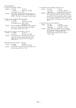
11. Tape Speed Adjustment (DECK 2)
Settings : Test tape :
TTA100
Test point :
TP8 (Lch), TP9 (Rch)
Adjustment location : SFR1
Method : Play back the test tape and adjust SFR1 so that the
test point becomes 3000 Hz ± 5 Hz (FWD) and FWD
SPEED ± 45Hz (REV) with respect to forward speed.
12. Head Azimuth Adjustment (DECK 1, DECK 2)
Settings : Test tape :
TTA330
Test point :
TP8 (Lch), TP9 (Rch)
Adjustment location : Head azimuth
adjustment screw
Method : Play back (FWD) the 8 kHz signal of the test tape and
adjust screw so that the output becomes maximum.
Next, perform on REV PLAY mode.
13. PB Frequency Response Check (DECK 1, DECK 2)
Settings : Test tape :
TTA330
Test point :
TP8 (Lch), TP9 (Rch)
Method : Play back the 315 Hz and 8 kHz signals of the test
tape and check that the output ratio of the 8 kHz
signal with respect to that of the 315 Hz signal is
0 dB ± 3 dB.
14. PB Sensitivity Check (DECK 1, DECK 2)
Settings : Test tape :
TTA200
Test point :
TP8 (Lch), TP9 (Rch)
Method : Play back the test tape and check that the output level
of the test point is 110 mV ± 3 dB.
15. REC/PB Frequency Response Check (DECK 2)
Settings : Test tape :
TTA602
Test point :
TP8 (Lch), TP9 (Rch)
Input signal :
8 kHz/1 kHz (-20 VU / 0dB)
Method : Apply a 1 kHz signal and REC mode. Then adjust
OSC attenuator so that the output level at TP8, TP9
becomes 10 mV. Record and play back the 1 kHz and
8 kHz signals and check that the output of the 8 kHz
signal is 0 dB ± 5 dB with respect to that of the 1 kHz
signal.
16. REC/PB Sensitivity Check (DECK 2)
Settings : Test tape :
TTA602
Test point :
TP8 (Lch), TP9 (Rch)
Input signal :
8 kHz (0VU / 0 dB)
Method : Apply a 8 kHz signal and REC mode. Then adjust
OSC attenuator so that the output level at TP8, TP9
becomes 100 mV. Record and play back
the 8 kHz signal and check that the output is
1 dB ± 3.5 dB.
Содержание NSX-VC220
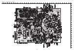
Страница 12: ... 12 SCHEMATIC DIAGRAM 1 MAIN 1 2 ...
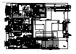
Страница 13: ... 13 SCHEMATIC DIAGRAM 2 FRONT DECK ...
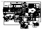
Страница 14: ... 14 SCHEMATIC DIAGRAM 3 TUNER ...
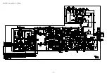
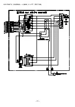
Страница 15: ... 15 SCHEMATIC DIAGRAM 4 MAIN 2 2 PT SECTION ...
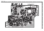
Страница 17: ... 17 SCHEMATIC DIAGRAM 5 AMP ...
Страница 19: ... 19 IC BLOCK DIAGRAM ...
Страница 20: ... 20 FL HNA 10SS19T GRID ASSIGNMENT ANODE PIN CONNECTION GRID ASSIGNMENT ANODE CONNECTION PIN CONNECTON ...
Страница 33: ...2 11 IKENOHATA 1 CHOME TAITO KU TOKYO 110 JAPAN TEL 03 3827 3111 Printed in Singapore 9301978 9720501 921338 ...

