12
11
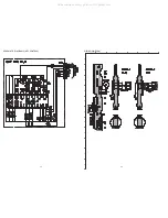
DECK C.B
82-ZM3-601-019 RBN-CORD,4P-75
CON105 87-099-756-019 CONN,15P 9604S F
SOL1 82-ZM1-618-310 SOL ASSY,27
SOL2 82-ZM1-626-010 SOL ASSY,27K
SFR1 87-024-581-010 SFR,3.3K DIA 6H
SW1 87-036-378-010 SW,PUSH 1-1-1 SH2
SW2 87-036-378-010 SW,PUSH 1-1-1 SH2
SW3 87-036-378-010 SW,PUSH 1-1-1 SH2
SW4 87-036-378-010 SW,PUSH 1-1-1 SH2
SW5 87-036-378-010 SW,PUSH 1-1-1 SH2
SW6 87-036-378-010 SW,PUSH 1-1-1 SH2
SW8 87-036-378-010 SW,PUSH 1-1-1 SH2
SW9 87-036-378-010 SW,PUSH 1-1-1 SH2
HEAD-1 C.B
HEAD-2 C.B
CON351 87-NF6-616-010 CONN ASSY,8P RPB
REF. NO
PART NO.
KANRI
DESCRIPTION
NO.
•
Regarding connectors, they are not stocked as they are not the initial order items.
The connectors are available after they are supplied from connector manufacturers upon the order is received.
8 8
A
Resistor Code
Chip Resistor Part Coding
Figure
Value of resistor
Chip resistor
Wattage
Type
Tolerance
1/16W
1/10W
1/8W
1608
2125
3216
5%
5%
5%
CJ
CJ
CJ
Form
L
W
t
1.6
0.8
0.45
2
1.25
0.45
3.2
1.6
108
118
128
: A
: A
CHIP RESISTOR PART CODE
0.55
Resistor Code
Dimensions (mm)
Symbol
1/16W
1005
5%
CJ
1.0
0.5
0.35
104
L
t
W
TRANSISTOR ILLUSTRATION
BCE
ECB
ECB
B
E
C
2SB1342
2SB1344
2SB1370
2SD2025
2SK2158
2SA1585
CC5551
CSC4115
KTA1266
KTC3198
KTC3199
2SA933S
DTC114ES
2SA1235
2SA1514
2SC2714
2SC3052
2SC3906
2SD1306
CMBT5551
CSD1306
DTA123EK
DTA143EK
KTA1298
RT1N141C
RT1P141C
RT1P144C
RT1P441C
G
S
D
2SK543
S
D
G
2SK360
D
G
S
GDS
2SK3053
BCE
FN1016
FP1016
All manuals and user guides at all-guides.com
all-guides.com
Содержание NSX-L980
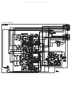
Страница 12: ...14 13 BLOCK DIAGRAM 1 MAIN All manuals and user guides at all guides com ...
Страница 13: ...15 BLOCK DIAGRAM 2 TUNER All manuals and user guides at all guides com ...
Страница 14: ...16 1 2 3 4 5 6 7 A B C D E F G H I J K WIRING 1 TUNER All manuals and user guides at all guides com ...
Страница 15: ...17 SCHEMATIC DIAGRAM 1 TUNER 18 All manuals and user guides at all guides com ...
Страница 17: ...21 SCHEMATIC DIAGRAM 2 DECK 22 All manuals and user guides at all guides com ...
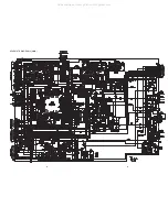
Страница 19: ...25 SCHEMATIC DIAGRAM 4 MAIN 26 All manuals and user guides at all guides com ...
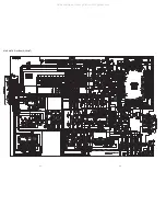
Страница 20: ...27 SCHEMATIC DIAGRAM 5 FRONT 28 S19 All manuals and user guides at all guides com ...
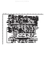
Страница 22: ...31 SCHEMATIC DIAGRAM 6 AMP 32 All manuals and user guides at all guides com ...
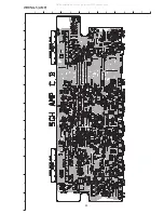
Страница 23: ...33 1 2 3 4 5 6 7 A B C D E F G H I J K WIRING 5 AMP All manuals and user guides at all guides com ...
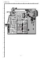
Страница 24: ...34 1 2 3 4 5 6 7 A B C D E F G H I J K WIRING 6 PT All manuals and user guides at all guides com ...
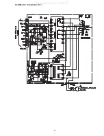
Страница 25: ...35 SCHEMATIC DIAGRAM 7 PT All manuals and user guides at all guides com ...
Страница 28: ...40 39 FL GRID ASSIGNMENT ANODE CONNECTION All manuals and user guides at all guides com ...
Страница 32: ...44 IC M62449FP IC M65847AFP All manuals and user guides at all guides com ...
Страница 33: ...45 IC LA1837NL IC LC72131D All manuals and user guides at all guides com ...


