


36
35
1
2
3
4
5
6
7
8
9
10
11
12, 13
14
15
16
17
18
19, 20
21
22
23
24-28
29
30
31
32, 33
34
35
36
37
38
39
40
41
42
DEFI
TAI
PDO
VVSS
ISET
VVDD
FR
VSS
EFMO
EFMIN
TEST2
CLV+, CLV–
___
V/P
HFL
TES
TOFF
TGL
JP+, JP–
PCK
FSEQ
VDD
SL+, SL–, CONT3-5
EMPH
C2F
DOUT
TEST3, TEST4
N.C.
MUTEL
LVDD
LCHO
LVSS
RVSS
RCHO
RVDD
MUTER
I
I
O
—
I
—
I
—
O
I
I
O
O
I
I
O
O
O
O
O
—
I/O
O
O
O
I
—
O
—
O
—
—
O
—
O
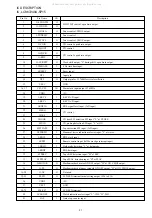
Defect sense signal (DEF) input pin. (Connect to 0V when not used).
Test signal input pin with built-in pull-down resistor. Be sure to connect to 0V.
Phase comparator output pin to control external VCO.
For PLL.
GND pin for built-in VCO. Be sure to connect to 0V.
Pin to which external resistor adjusting the PD0 output current.
Power supply pin for built-in VCO.
Pin for VCO frequency range adjustment.
Digital system GND. Be sure to connect to 0V.
For slice level control.
EFM signal output pin.
EFM signal input pin.
Test signal input pin with built-in pull-down resistor. Be sure to connect to 0V.
Disc motor control output. Three level output is possible using command.
Rough servo or phase control automatic selection monitoring output pin. Rough servo
at H. Phase servo at L.
Track detect signal input pin. Schmidt input.
Tracking error signal input pin. Schmidt input.
Tracking OFF output pin.
Tracking gain selection output pin. Gain boost at L.
Track jump control signal output pin. Three level output is possible using command.
EFM data playback clock monitoring pin 4.3218 MHz when phase is locked in.
Sync signal detection output pin. H when the sync signal which is detected from EFM
signal and thesync signal which is internally generated agree.
Digital system power supply pin.
The pin is controlled by the serial data
command from microprocessor. When
General purpose input/output pin 1 to 5.
the pin is not used, set the pin to the input
terminal and connect to 0V, or alternately
set the pin to output terminal and leave
the pin open.
De-emphasis monitor output pin. De-emphasis disc is being played back at H.
C2 flag output pin.
DIGITAL OUT output pin. (EIAJ format).
Test signal input pin with built-in pull-down resistor. Be sure to connect to 0V.
Not used. Set the pin to open.
L-channel mute output pin.
L-channel 1-bit DAC.
L-channel power supply pin.
L-channel output pin.
L-channel GND. Be sure to connect to 0V.
R-channel GND. Be sure to connect to 0V.
R-channel 1-bit DAC.
R-channel output pin.
R-channel power supply pin.
R-channel mute output pin.
IC, LC78622ED
Pin No.
Pin Name
I/O
Description
43
44
45
46
47
48
49
50
51
52
53
54
55
56
57
58
59
60
61
62
63
64
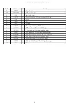
XVDD
XOUT
XIN
XVSS
SBSY
EFLG
PW
SFSY
SBCK
FSX
WRQ
RWC
SQOUT
COIN
___________
CQCK
________
RES
TST11
16M
4.2M
TEST5
______
CS
TEST1
—
O
I
—
O
O
O
O
I
O
O
I
O
I
I
I
O
O
O
I
I
I
Crystal oscillator power supply pin.
Pin to which external 16.9344 MHz crystal oscillator is connected.
Crystal oscillator GND pin. Be sure to connect to 0V.
Subcode block sync signal output pin.
C1, C2, single and dual correction monitoring pin.
Subcode P, Q, R, S, T, U and W output pin.
Subcode frame sync signal output pin. Falls down when subcode enters standby.
Subcode read clock input pin. Schmidt input. (Be sure to connected to 0V when not
in use.)
Pin outputting the 7.35 kHz sync signal which is generated by dividing frequency of
crystal oscillator.
Subcode Q output standby output pin.
Read/write control input pin. Schmidt input.
Subcode Q output pin.
Command input pin from microprocessor.
Command input read clock or subcode read input clock from SQOUT pin
LC78622 reset input pin. Set this pin to L once when the main power is turned on.
Test signal output pin. Use this pin as open (normally L output).
16.9344 MHz output pin.
4.2336 MHz output pin.
Test signal input pin with built-in pull-down resistor. Be sure to connect to 0V.
Chip select signal input pin with built-in pull-down resistor. Be sure to connect to 0V
while it is not controlling.
Test signal input pin without built-in pull-down resistor. Be sure to connect to 0V.
Note:
The same potential must be applied to the respective power supply terminals. (VDD, VVDD, LVDD, RVDD, XVDD)
Pin No.
Pin Name
I/O
Description
All manuals and user guides at all-guides.com
Содержание LCX-157 HS
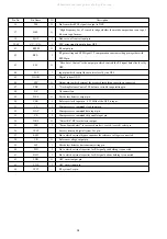
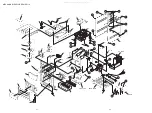
Страница 14: ...22 21 SCHEMATIC DIAGRAM 3 FRONT IRDDT IR200 All manuals and user guides at all guides com ...
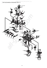
Страница 15: ...24 23 SCHEMATIC DIAGRAM 4 CD All manuals and user guides at all guides com ...
Страница 16: ...26 25 VOLTAGE CHART All manuals and user guides at all guides com a l l g u i d e s c o m ...
Страница 17: ...28 27 All manuals and user guides at all guides com ...
Страница 18: ...30 29 ELECTRICAL ADJUSTMENT All manuals and user guides at all guides com ...


