Aiwa CSD-EL300 EZ(S) Скачать руководство пользователя страница 34

2–11, IKENOHATA 1–CHOME, TAITO-KU, TOKYO 110, JAPAN  TEL:03 (3827) 3111

737004

Printed in Singapore

Содержание CSD-EL300 EZ(S)

Страница 1: ...SERVICE MANUAL D A T A COMPACT DISC STEREO RADIO CASSETTE RECORDER CSD EL300 S M Code No 09 003 344 1N1 US BASIC TAPE MECHANISM 2ZM 1YR7NC BASIC CD MECHANISM 3ZG 3 E2NC...

Страница 2: ...ign and specifications are subject to change without notice REF NO PART NO KANRI DESCRIPTION NO ACCESSORIES PACKAGE LIST 1 8A CH2 903 010 IB U ESF FM 2 8A CH2 950 010 RC UNIT ACH 2 3 87 A80 027 010 AC...

Страница 3: ...ceux sp cifi s peut entra ner une dangereuse exposition aux radiations ADVARSEL Usynlig laserst ling ved bning n r sikkerhedsafbrydereer ude af funktion Undg uds ttelse for str ling This Compact Disc...

Страница 4: ...134 080 CAPACITOR TC U 0 01 16 C241 87 010 401 080 CAP ELECT 1 50V C242 87 010 401 080 CAP ELECT 1 50V C243 87 010 401 080 CAP ELECT 1 50V C244 87 010 401 080 CAP ELECT 1 50V C245 87 010 401 080 CAP E...

Страница 5: ...ECT 220 10V C463 87 018 134 080 CAPACITOR TC U 0 01 16 C465 87 010 404 080 CAP ELECT 4 7 50V C466 87 018 209 080 CAP CER 0 1 50V C467 87 010 263 080 CAP ELECT 100 10V C468 87 018 119 080 CAP CER 100P...

Страница 6: ...0P 50 CH C618 87 010 197 080 CAP CHIP 0 01 DM C619 87 010 197 080 CAP CHIP 0 01 DM C620 87 018 044 080 CAP TC S 1000P 50 B C620 87 010 178 080 CHIP CAP 1000P C621 87 010 405 080 CAP ELECT 10 50V C622...

Страница 7: ...CJ CJ Form L W t 1 6 0 8 0 45 2 1 25 0 45 3 2 1 6 108 118 128 A A CHIP RESISTOR PART CODE 0 55 Resistor Code Dimensions mm Symbol 1 16W 1005 5 CJ 1 0 0 5 0 35 104 L t W E B C E C B E C B ECB ECB ECB 2...

Страница 8: ...8 LCD DISPLAY LCD AIW4213...

Страница 9: ...10 9 SCHEMATIC DIAGRAM 1 MAIN...

Страница 10: ...12 11 SCHEMATIC DIAGRAM 2 CD MAIN...

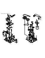
Страница 11: ...1 2 3 4 5 6 7 8 9 10 11 12 13 14 A B C D E F G H I J K 14 13 WIRING 1 MAIN CD MAIN...

Страница 12: ...16 15 1 2 3 4 5 6 7 A B C D E F G H I J K WIRING 2 PWR BATT F705 D 2 5A T 250V U JW 1 2 3 4 5 6 7 A B C D E F G H I J K WIRING 3 TU...

Страница 13: ...18 17 SCHEMATIC DIAGRAM 3 TU R005 C026 2 8 4 1 0 3 9 0 0 2 0 TU 4 7 OTHER 0 7 8 2 3 0 2 3 0 8 4 5 0 1 2 4 5 4 7 4 2 4 7 0 0 4 1 3 1 3 4 8 4 6 4 8 3 0 0 4 7 0 9 1 0 0 7...

Страница 14: ...20 19 SCHEMATIC DIAGRAM 4 FRONT SOL2...

Страница 15: ...1 2 3 4 5 6 7 8 9 10 11 12 13 14 A B C D E F G H I J K 22 21 WIRING 4 FRONT...

Страница 16: ...ation Azimuth adjustment screw Method Play back the test tape and adjust so that the output is maximum PRACTICAL SERVICE FIGURE TUNER SECTION FM SECTION IHF Sensitiviy Less than 18dB THD 3 at 98MHz Si...

Страница 17: ...25 IC BLOCK DIAGRAM IC TA2149N IC LC72121M...

Страница 18: ...16 15 14 13 12 11 10 9 8 7 6 5 4 3 2 1 CONT VSS OUT2 TONEL2 TONEH2 QF3 QF4 INB2 INA2 INC2 IND2 INE2 VDD GND OUT1 TONEL1 TONEH1 QF2 QF1 INB1 INA1 INC1 IND1 INE1 MUTE Mono SW VOL VOL Treble boost Bass...

Страница 19: ...27 IC LA6541D...

Страница 20: ...on constants are connected between the TD and VR pins Tracking phase compensation setting pin Tracking jump signal kick pulse amplitude setting pin Tracking control signal output pin Focusing control...

Страница 21: ...he DSP Digital system GND Output pin to which external focus search smoothing capacitor is connected Tracking Balance Control EF balance variable range setting pin No connection Disc defect detector o...

Страница 22: ...vo or phase control automatic selection monitoring output pin Rough servo at H Phase servo at L Track detect signal input pin Schmidt input Tracking error signal input pin Schmidt input Tracking OFF o...

Страница 23: ...in Schmidt input Be sure to connected to 0V when not in use Pin outputting the 7 35 kHz sync signal which is generated by dividing frequency of crystal oscillator Subcode Q output standby output pin R...

Страница 24: ...l settings output SW Not connected LCD segment output and initial settings output LW Not connected LCD segment output and initial settings output MW 10K LCD segment output and initial settings output...

Страница 25: ...GND Power supply for microcomputer 5V CD PWR control output TU PWR control output Power supply control output Not connected Main mute output FM force control MONO output Not connected BEAT switch over...

Страница 26: ...20 8A CH2 620 010 FF CABLE 10P 1 25 21 8A CH2 619 010 FF CABLE 14P 1 25 22 82 ZM1 263 110 LVR EJECT L 23 8A CH2 009 010 WINDOW CASS 24 8A CH2 003 010 BOX CASS 25 8A CH2 206 010 SPR T CASS 26 8A CH2 0...

Страница 27: ...10 11 12 13 14 15 16 17 18 19 LCD P C B P C B P C B P C B P C B P C B 20 21 22 23 24 25 26 27 28 29 30 31 32 33 34 36 37 38 39 40 41 42 43 44 45 46 49 47 a 48 35 a b b B B B C C C C C B A B B D D D G...

Страница 28: ...EW 1 1 1 A A 56 16 15 14 30 13 12 11 10 17 19 4 6 20 5 22 21 23 25 26 29 29 27 28 3 2 RELAY C B HLDR WIRE 3 B B A 18 9 7 A B A B 31 38 39 40 32 34 33 35 43 45 41 41 37 44 52 51 55 50 DECK C B SOL2 49...

Страница 29: ...T PINCH R 29 82 ZM1 240 110 LVR REC 30 82 ZM1 298 010 SPR P EARTH 31 82 ZM1 255 310 SPR E LVR DIR 32 82 ZM1 221 110 GEAR CAM 33 82 ZM1 227 210 LVR TRIG 34 82 ZM1 224 410 LVR FR 35 86 ZM4 201 010 SPR...

Страница 30: ...40 CD MECHANISM EXPLODED VIEW 1 1 B C A B C 3 MOTOR 2 C B 2 4 5 6 7 8 9 10 11 12 1 17 3ZG2 17 CUSH G MAIN A B D D A CUSH G MAIN A A 16 14 15 13 C C...

Страница 31: ...207 010 GEAR TRAY 7 83 ZG3 204 210 GEAR C 8 83 ZG3 205 010 GEAR D 9 83 ZG3 217 010 S SCREW GEAR D 10 83 ZG3 220 210 GEAR PULLEY 2 11 83 ZG3 214 010 BELT L 12 83 ZG3 229 410 TRAY CD 2 13 83 ZG3 210 11...

Страница 32: ...86 ZM4 201 010 SPR E TRIG 3 82 ZM1 255 310 SPR E LER DIR 82 ZM1 258 110 SPR T PINCH L 82 ZM1 213 010 SPR T HEAD 82 ZM1 269 010 SPR T BRG 82 ZM1 214 010 SPR T DIR 82 ZM1 285 410 SPR C BT L 82 ZM3 323 0...

Страница 33: ...ISTOR TRIMMER CAP TRIMMER TUN CAP VARIABLE CAPACITOR VIB CER RESONATOR CERAMIC VIB XTAL RESONATOR CRYSTAL VR VOLUME ZENER DIODE ZENER REFERENCE NAME LIST MECHANICAL SECTION DESCRIPTION REFERENCE NAME...

Страница 34: ...2 11 IKENOHATA 1 CHOME TAITO KU TOKYO 110 JAPAN TEL 03 3827 3111 737004 Printed in Singapore...

Отзывы: