


30
1
2
3
4
5
6
7
8
9
10
11
12, 13
14
15
16
17
18
19, 20
21
22
23
24
25
26
27
28
29
30
31
32, 33
34
35
36
37
38
39
40
41
42
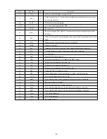
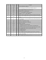
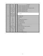
Pin No.
Pin Name
I/O
Description
DEFI
TAI
PDO
VVSS
ISET
VVDD
FR
VSS
EFMO
EFMIN
T2
CLV+, CLK-
___
V/P
HFL
TES
TOFF
TGL
JP+, JP-
PCK
FSEQ
VDD
SL+
SL-
—
PUIN
RW
EMPH
C2F
DOUT
T3, T4
N.C.
MUTEL
LVDD
LCHO
LVSS
RVSS
RCHO
RVDD
MUTER
I
I
O
—
I
—
I
—
O
I
I
O
O
I
I
O
O
O
O
O
—
O
O
—
I
O
O
O
O
I
—
O
—
O
—
—
O
—
O
Defect sense signal (DEF) input pin. (Connect to 0V when not used).
Test signal input pin with built-in pull-down resistor. Be sure to connect to 0V.
Phase comparator output pin to control external VCO.
For PLL.
GND pin for built-in VCO. Be sure to connect to 0V.
Pin to which external resistor adjusting the PD0 output current.
Power supply pin for built-in VCO.
Pin for VCO frequency range adjustment.
Digital system GND. Be sure to connect to 0V.
For slice level control.
EFM signal output pin.
EFM signal input pin.
Test signal input pin with built-in pull-down resistor. Be sure to connect to 0V.
Disc motor control output. Three level output is possible using command.
Rough servo or phase control automatic selection monitoring output pin. Rough servo
at H. Phase servo at L.
Track detect signal input pin. Schmidt input.
Tracking error signal input pin. Schmidt input.
Tracking OFF output pin.
Tracking gain selection output pin. Gain boost at L.
Track jump control signal output pin. Three level output is possible using command.
EFM data playback clock monitoring pin 4.3218 MHz when phase is locked in.
Sync signal detection output pin. H when the sync signal which is detected from EFM
signal and thesync signal which is internally generated agree.
Digital system power supply pin.
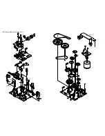
Moves the sled to outer circumference.
Moves the sled to inner circumference.
Not connected.
CD pickup inner switch detection.
Read, wright signal.
De-emphasis monitor output pin. De-emphasis disc is being played back at H.
C2 flag output pin.
DIGITAL OUT output pin. (EIAJ format).
Test signal input pin with built-in pull-down resistor. Be sure to connect to 0V.
Not used. Set the pin to open.
L-channel mute output pin.
L-channel 1-bit DAC.
L-channel power supply pin.
L-channel output pin.
L-channel GND. Be sure to connect to 0V.
R-channel GND. Be sure to connect to 0V.
R-channel 1-bit DAC.
R-channel output pin.
R-channel power supply pin.
R-channel mute output pin.
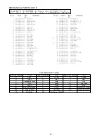
IC, LC78622ED
Содержание CSD-EL300 EZ(S)
Страница 8: ...8 LCD DISPLAY LCD AIW4213...
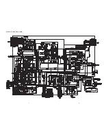
Страница 9: ...10 9 SCHEMATIC DIAGRAM 1 MAIN...
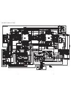
Страница 10: ...12 11 SCHEMATIC DIAGRAM 2 CD MAIN...
Страница 11: ...1 2 3 4 5 6 7 8 9 10 11 12 13 14 A B C D E F G H I J K 14 13 WIRING 1 MAIN CD MAIN...
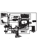
Страница 14: ...20 19 SCHEMATIC DIAGRAM 4 FRONT SOL2...
Страница 15: ...1 2 3 4 5 6 7 8 9 10 11 12 13 14 A B C D E F G H I J K 22 21 WIRING 4 FRONT...
Страница 17: ...25 IC BLOCK DIAGRAM IC TA2149N IC LC72121M...
Страница 19: ...27 IC LA6541D...
Страница 34: ...2 11 IKENOHATA 1 CHOME TAITO KU TOKYO 110 JAPAN TEL 03 3827 3111 737004 Printed in Singapore...