Diagrams 139
Table 6-1. Signal Name Descrptions (continued)
Signal Name
Description
ROM*
Read only memory chip select
SPCLR
Secondary power clear
SRQ
Service request (GPIB)
SRX
Secondary receive serial data
STX
Secondary transmit serial data
THERM AMB
Ambient temperature
THERM HS
Heat sink temperature
UART*
Universal asynchronous receive/transmit chip select signal
VMON
Voltage monitor
VOS
Voltage offset
VPROG
Voltage programming
WR*
Write
15 ISUP
15 volt supply is up (has stabilized)
Test Points
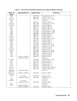
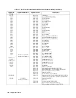
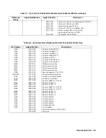
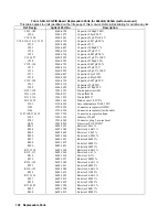
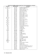
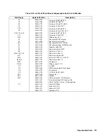
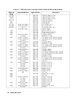
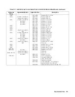
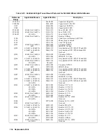
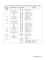
Table 6-3 lists the test points that appear on the schematic and component location diagrams. The table includes the test
point (e.g.,
, the circuit point (AlU608-l5), and the signal name (CV). The "Measurement and Conditions" column
gives signal measurements and the conditions (e.g., operating mode) required to obtain the measurement. Where
measurements differ, the applicable models are specified in the table. The following table list summary information about
notes appearing in schematic diagrams.
Table 6-2. General Schematic Notes:
1. All resistors are in ohms +1% 1/8 W, unless otherwise specified.
2. All capacitors are in microfarads unless otherwise specified.
3. Signal lines that are terminated by flags continue on other sheets, and may also go to other locations on the same sheet.
Example: CVPROG (SH.2 8C); "SH.2 8C" indicates the sheet number and the coordinates on that sheet where the
CVPROG signal line goes.
4. Unterminated signal lines go to at least one other location on the same sheet.
Example: _PRX (3A) where "3A" indicates the coordinates on this schematic sheet where the PRX signal line goes.
5. Unless otherwise noted, bias connections to integrated-circuit packages are as follows:
Common
+ 5V
14-pin packages
pin 7
pin 14
16-pin packages
pin 8
pin 16
20-pin packages
pin 10
pin 20
Содержание 6541A
Страница 12: ...12 Verification Figure 2 1 Basic Test Setup CV TESTS CV TESTS ...
Страница 18: ...18 Verification Figure 2 3 CC RMS Noise Measurement Test Setup ...
Страница 30: ......
Страница 32: ...32 Troubleshooting Figure 3 1 Top View with Cover Removed for 655xA 665xA Models Sheet 1 of 2 ...
Страница 33: ...Troubleshooting 33 Figure 3 1 Top View with Cover Removed for 655xA 665xA Models Sheet 2 of 2 ...
Страница 37: ...Troubleshooting 37 Figure 3 2 Overall Troubleshooting Flow Diagram Sheet 1 of 4 ...
Страница 38: ...38 Troubleshooting Figure 3 2 Overall Troubleshooting Flow Diagram Sheet 2 of 4 ...
Страница 39: ...Troubleshooting 39 Figure 3 2 Overall Troubleshooting Flow Diagram Sheet 3 of 4 ...
Страница 40: ...40 Troubleshooting Figure 3 2 Overall Troubleshooting Flow Diagram Sheet 4 of 4 ...
Страница 43: ...Troubleshooting 43 Figure 3 4 Connections For A2 GPIB Board Models 664xA 665xA Only Sheet 1 of 3 ...
Страница 44: ...44 Troubleshooting Figure 3 4 Connections For A2 GPIB Board Models 664xA 665xA Only Sheet 2 of 3 ...
Страница 45: ...Troubleshooting 45 Figure 3 4 Connections For A2 GPIB Board Models 664xA 665xA Only Sheet 3 of 3 ...
Страница 51: ...Troubleshooting 51 Figure 3 5 No Display Troubleshooting ...
Страница 52: ...52 Troubleshooting Figure 3 6 OV Will Not Fire Troubleshooting ...
Страница 53: ...Troubleshooting 53 Figure 3 7 OV At Turn On Troubleshooting Sheet 1 of 2 ...
Страница 54: ...54 Troubleshooting Figure 3 7 OV At Turn On Troubleshooting Sheet 2 of 2 ...
Страница 55: ...Troubleshooting 55 Figure 3 8 Output Held Low Troubleshooting Sheet 1 of 2 ...
Страница 56: ...56 Troubleshooting Figure 3 8 Output Held Low Troubleshooting Sheet 2 of 2 ...
Страница 57: ...Troubleshooting 57 Figure 3 9 Output Held High Troubleshooting ...
Страница 58: ...58 Troubleshooting Figure 3 10 DAC Circuits Troubleshooting ...
Страница 59: ...Troubleshooting 59 Figure 3 11 DAC Waveforms Figure 3 12 CV CC DAC and Amplifier Troubleshooting ...
Страница 60: ...60 Troubleshooting Figure 3 13 Serial Down Troubleshooting Sheet 1 of 2 ...
Страница 61: ...Troubleshooting 61 Figure 3 13 Serial Down Troubleshooting Sheet 2 of 2 ...
Страница 62: ...62 Troubleshooting Figure 3 14 Secondary Down Troubleshooting Sheet 1 of 2 ...
Страница 63: ...Troubleshooting 63 Figure 3 14 Secondary Down Troubleshooting Sheet 2 of 2 ...
Страница 64: ...64 Troubleshooting Figure 3 15 Slow Down Programming Troubleshooting ...
Страница 65: ...Troubleshooting 65 Figure 3 16 Isolator Board Circuits Troubleshooting ...
Страница 73: ...Troubleshooting 73 Figure 3 18 Location of Cable and Connector Locations for 655xA and 665xA Models Only ...
Страница 80: ......
Страница 87: ...Principles of Operation 87 Figure 4 4 Output Power and Control Circuits ...
Страница 94: ......
Страница 136: ......
Страница 145: ...Figure 6 1 Power Supply Interconnection Diagram for All Models ...
Страница 146: ...Figure 6 2 AC Power Distribution Diagram for 655xA 665xA Models ...
Страница 147: ...Figure 6 3 GPIB Board Assembly Diagram sheet 1 of 2 ...
Страница 148: ...2 3 4 1 6 5 7 8 Figure 6 3 GPIB Board Schematic Diagram sheet 2 of 2 ...
Страница 149: ...Figure 6 4 Front Panel Board Assembly Diagram sheet 1 of 2 ...
Страница 150: ...Figure 6 4 Front Panel Board Schematic Diagram sheet 2 of 2 ...
Страница 152: ...Figure 6 5 A1 Main Board Assembly Diagram for 654xA 664xA Models Only ...
Страница 159: ...49 50 47 48 51 53 52 57 56 55 54 Figure 6 6 Left Tunnel Circuits Schematic Diagram for 655xA 665xA Models Only sheet 1 ...
Страница 160: ...Figure 6 6 Left Tunnel Circuits Schematic Diagram for 654xA 664xA Models Only sheet 2 ...
Страница 161: ...58 59 60 61 62 63 Figure 6 7 Right Tunnel Circuits Schematic Diagram for 655xA 665xA Models Only sheet 1 ...
Страница 162: ...Figure 6 7 Right Tunnel Circuits Schematic Diagram for 654xA 664xA Models Only sheet 2 ...
Страница 164: ......
Страница 165: ...Figure 6 9 Power Transformer Wiring Diagram for Models 655xA and 665xA Sheet 1 of 3 Diagrams 165 ...
Страница 166: ...Figure 6 9 Power Transformer Wiring Diagram for Models 655xA and 665xA Sheet 2 of 3 166 Diagrams ...
Страница 167: ...Figure 6 9 Power Transformer Wiring Diagram for Models 655xA and 665xA Sheet 3 of 3 Diagrams 167 ...
Страница 168: ......

