background image

33

Chapter 3  

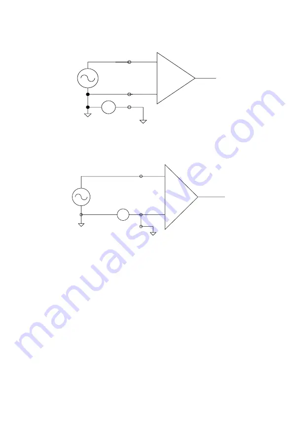
Correct Connection

Incorrect Connection

Expanding Analog Inputs

You can expand any or all of the PCL-818HD/HG/L's A/D input channels 
using multiplexing daughterboards. Daughterboards without D-type con-
nectors require the PCLD-774 Analog Expansion Board.
The PCLD-789(D) Amplifier and Multiplexer multiplexes 16 differential 
inputs to one A/D input channel. You can cascade up to eight PCLD-
789(D)s to the PCL-818HD/HG/L for a total of 128 channels. See the 
PCLD-789(D) user's manual for complete operating instructions.
The PCLD-774 Analog Expansion Board accommodates multiple exter-
nal signal-conditioning daughter boards, such as PCLD-779 and PCLD-
789(D). It features five sets of on-board 20-pin header connectors. A spe-
cial star-type architecture lets you cascade multiple signal-conditioning 
boards without the signal-attenuation and current-loading problems of 
normal cascading.


+

-

HIGH

LOW

 +

Vin

 -

 +

Vs

 -

Vcm

GND

Vin=Vs

+

-

+

-

 +

Vs

 -

Vcm

HIGH

LOW

GND

 +

Vin


-

Vin=Vs+Vcm

+

-

Содержание PCL-818 Series

Страница 1: ...PCL 818 Series 12 bit ISA Multifunction Card User Manual ...

Страница 2: ... by any means without the prior written permission of Advantech Co Ltd Information provided in this manual is intended to be accurate and reli able However Advantech Co Ltd assumes no responsibility for its use nor for any infringements of the rights of third parties which may result from its use Acknowledgements Intel and Pentium are trademarks of Intel Corporation Microsoft Windows and MS DOS ar...

Страница 3: ...placement materials service time and freight Please consult your dealer for more details If you think you have a defective product follow these steps 1 Collect all the information about the problem encountered For example CPU speed Advantech products used other hardware and software used etc Note anything abnormal and list any onscreen messages you get when the problem occurs 2 Call your dealer an...

Страница 4: ...p 1 Visit the Advantech web site at www advantech com support where you can find the latest information about the product Step 2 Contact your distributor sales representative or Advantech s cus tomer service center for technical support if you need additional assistance Please have the following information ready before you call Product name and serial number Description of your peripheral attachm...

Страница 5: ...r cord so that people cannot step on it Do not place anything over the power cord 10 All cautions and warnings on the equipment should be noted 11 If the equipment is not used for a long time disconnect it from the power source to avoid damage by transient overvoltage 12 Never pour any liquid into an opening This may cause fire or elec trical shock 13 Never open the equipment For safety reasons th...

Страница 6: ... REPLACE ONLY WITH THE SAME OR EQUIVALENT TYPE RECOMMENDED BY THE MANUFACTURER DISCARD USED BATTERIES ACCORD ING TO THE MANUFACTURER S INSTRUCTIONS The sound pressure level at the operator s position according to IEC 704 1 1982 is no more than 70 dB A DISCLAIMER This set of instructions is given according to IEC 704 1 Advantech disclaims all responsibility for the accuracy of any statements contai...

Страница 7: ...Figure 2 4 Device Settings 17 Figure 2 5 Device Name 18 Figure 2 6 Test Utility 19 Chapter 3 Signal Connections 22 3 1 Overview 22 3 2 Switch Jumper Settings 22 Figure 3 1 Connectors Jumpers Switches 22 3 3 Signal Connections 30 3 3 1 Pin Assignments 30 3 3 2 I O Connector Signal Description 31 Figure 3 2 Analog Output Connections 34 3 4 Field Wiring Considerations 36 Appendix A Specifications 38 ...

Страница 8: ...BASE 06H 54 C 11 Clear Interrupt Request BASE 08H 55 C 12 A D Status BASE 08H 55 C 13 A D Control BASE 09H 57 C 14 Timer Counter Enable BASE 0AH 59 C 15 Programmable Timer Counter BASE 0C 0FH 59 C 16 Clear FIFO Interrupt Request BASE 14H 60 C 17 A D Data and Channel from FIFO BASE 17 18H 60 C 18 FIFO Status BASE 19H 61 C 19 FIFO Clear BASE 19H 62 Appendix D Calibration 64 D 1 VR Assignment 65 Figu...

Страница 9: ...2 CHAPTER 1 Overview Sections include Introduction Features Applications Installation guide Software Overview Device Driver Roadmap Accessories ...

Страница 10: ...er and pre dictable performance under Windows Automatic channel scanning circuitry and on board SRAM let you per form multiple channel A D conversion with DMA and individual gains for each channel The PCL 818HD uses a CPLD chip designed in house by Advantech engineers This single chip integrates most of the card s functions giving you maximum accuracy and reliability along with minimum cost size a...

Страница 11: ...ers the following main features Automatic Channel Gain Scanning The PCL 818HD HG L features an automatic channel gain scanning cir cuit This circuit instead of your software controls multiplexer switching during sampling On board SRAM stores different gain values for each channel This combination lets you perform multi channel high speed sampling up to 100 KHz with different gains for each channel...

Страница 12: ...P Switch that helps define each card s ID when multiple PCL 818HD HG L cards have been installed on the same PC chassis The board ID setting function is very useful when users build their system with multiple PCL 818HD HG L cards With correct Board ID settings you can easily identify and access each card during hardware configuration and software programming Note For detailed specifications of the...

Страница 13: ...5 785B 786 788 789D 880 885 8115 optional PC or workstation with a PCI bus slot Win 95 98 NT 2000 ME XP Some other optional components are available for enhanced operation Application software ActiveDAQ GeniDAQ or 3rd party software After you get the necessary components and maybe some of the accesso ries for enhanced operation of your Multifunction card you can then begin the Installation procedu...

Страница 14: ...PCL 818 Series User Manual 6 Figure 1 1 Installation Flow Chart ...

Страница 15: ... at no extra charge It also comes with all the Advantech DA C cards Advantech s Device Drivers features a complete I O function library to help boost your application performance The Advantech Device Drivers for Windows 95 98 NT 2000 ME XP works seamlessly with development tools such as Visual C Visual Basic Borland C Builder and Borland Delphi Register level Programming Register level programming...

Страница 16: ...ce Drivers Manual for your reference Please refer to the corresponding sections in this chapter on the Device Drivers Manual to begin your programming efforts You can also look at the example source code provided for each programming tool since they can get you very well oriented The Device Drivers Manual can be found on the companion CD ROM Alternatively if you have already installed the Device D...

Страница 17: ...up direct I O Event Function Group For the usage and parameters of each function please refer to the Func tion Overview chapter in the Device Drivers Manual Troubleshooting Device Drivers Error Driver functions will return a status code when they are called to perform a certain task for the application When a function returns a code that is not zero it means the function has failed to perform its ...

Страница 18: ...s analog and digital lines are separately sheathed and shielded to neutralize EMI EMC problems Wiring Boards ADAM 3920 20 pin wiring terminal for DIN rail mounting ADAM 3937 37 pin D type wiring terminal for DIN rail mounting PCLD 7216 16 channel SSR I O module carrier board PCLD 780 Universal screw terminal board PCLD 782 16 channel opto isolated D I board PCLD 782B 24 channel opto isolated D I b...

Страница 19: ...2 CHAPTER 2 Installation Sections include Unpacking Driver Installation Hardware Installation Device Setup Configuration ...

Страница 20: ...damage Touch the metal part of your computer chassis with your hand to dis charge the static electricity accumulated on your body Alternatively one can also use a grounding strap Touch the anti static bag to a metal part of your computer chassis before opening the bag Take hold of the card only by the metal bracket when removing it out of the bag After taking out the card you should first Inspect ...

Страница 21: ... DA C card package Please follow the steps below to install the driver software Step 1 Insert the companion CD ROM into your CD ROM drive Step 2 The Setup program will be launched automatically if you have the autoplay function enabled on your system When the Setup Pro gram is launched you will see the following Setup Screen Figure 2 1 Advantech Automation Software Setup Note If the autoplay funct...

Страница 22: ...allation instructions step by step to complete your device driver installa tion and setup Figure 2 2 Options for Driver Setup For further information on driver related issues an online version of the Device Drivers Manual is available by accessing the following path Start Advantech Automation Device Manager Device Driver s Manual ...

Страница 23: ... edges and carefully align it with the slot Insert the card firmly into place Use of excessive force must be avoided other wise the card might be damaged Step 6 Fasten the bracket of the ISA card on the back panel rail of the computer with screws Step 7 Connect appropriate accessories 37 pin cable wiring terminals etc if necessary to the ISA card Step 8 Replace the cover of your computer chassis R...

Страница 24: ...PIs of Advantech Device Drivers Setting Up the Device Step 1 To install the I O device for your card you must first run the Device Installation program by accessing Start Advantech Auto mation Device Manager Advantech Device Manager Step 2 You can then view the device s already installed on your system if any on the Installed Devices list box Since you have not installed any device yet you might s...

Страница 25: ...onfiguring the Device Step 4 On the Device Setting dialog box Fig 2 4 you can configure the A D channels configuration either as 8 Differential or 16 Single ended and specify the D A voltage reference either as External or Internal Figure 2 4 Device Settings Step 5 After you have finished configuring the device click OK and the device name will appear in the Installed Devices box as seen below ...

Страница 26: ...PCL 818 Series User Manual 18 Figure 2 5 Device Name After your card is properly installed and configured you can click the Test button to test your hardware by using the testing utility supplied ...

Страница 27: ...19 Chapter2 Figure 2 6 Test Utility For more detailed information please refer to Chapter 2 of the Device Drivers Manual You can also find the rich examples on the CD ROM to speed up your programming ...

Страница 28: ...PCL 818 Series User Manual 20 ...

Страница 29: ...2 CHAPTER 3 Signal Connections Sections include Overview Switch Jumper Settings Signal Connections Field Wiring Considerations ...

Страница 30: ...eceiving data cor rectly A good signal connection can avoid unnecessary and costly dam age to your PC and other hardware devices This chapter provides useful information about how to connect input and output signals to the PCL 818HD HG L via the I O connector 3 2 Switch Jumper Settings The PCL 818HD HG L card has one function switch and five jumper set tings Figure 3 1 Connectors Jumpers Switches ...

Страница 31: ...he FIFO disabled Switch SW1 sets the card s base beginning address Valid base addresses range from Hex 000 to Hex 3F0 Other devices in your system may however be using some of these addresses We set the PCL 818HD HG L for a base address of Hex 300 at the fac tory If you need to adjust it to some other address range set switch SW1 as shown in the following table Switch 1 2 3 4 5 6 Line A9 A8 A7 A6 ...

Страница 32: ...t hand position marked S E for 16 single ended inputs Table 3 1 Switch SW2 Settings DMA Channel Selection JP7 The PCL 818HD HG L supports DMA data transfer Jumper JP7 selects the DMA channel 1 or 3 Table 3 2 Jumper JP7 Settings D A Reference Voltage Int Ext JP11 Jumper JP11 selects reference voltage source for the PCL 818HD HG L s D A converters You can use the card s internal reference or supply ...

Страница 33: ...n to function as the external reference The ref erence input can be either DC or AC 100 KHz When you use an external reference with voltage Vref you can program the D A channel to output from 0 V to Vref you can also use the D A converter as a programmable attenuator The attenuation factor between reference input and analog output is Attenuation factor G 4095 Where G is a value you write to the D ...

Страница 34: ...equency for the 8254 programmable clock timer You have two choices 10 MHz and 1 MHz This lets you generate pacer output frequencies from 2 5 MHz to 0 00023 Hz 71 minutes pulse The following equation gives the pacer rate Pacer rate Fclk Divl Div2 Fclk is 1 MHz or 10 MHz as set by jumper JP8 Div l and Div2 are the dividers set in counter 1 and counter 2 in the 8254 See Chapter 8 for more details Tab...

Страница 35: ... buffer you can only access the converted data from the A D output registers at BASE O 1 The PCL 818HD HG will only require 16 consecutive VO addresses Table 3 6 Jumper JP6 Settings Ext Trigger and Counter Gate 0 Control JP5 JP5 has two jumpers The upper jumper selects the card s A D trigger source when you use external triggering The lower jumper selects the gate control for counter 0 of the card...

Страница 36: ...18HD L s JPI to JP4 switch digital output channels O to 3 between the card s 20 pin connector and 37 pin connector If you set the jumpers to the left D side the digital output signals will come out on connector CN1 20 pin If you set the jumpers to the right S side the output signals will come out on connector CN3 37 pin These four digital output signals select the analog input channel when you use...

Страница 37: ...29 Chapter3 Table 3 8 Jumper Settings Jumpers Function Description JP1 first S0 D0 default JP1 second S1 D1 default JP1 third S2 D2 default JP1 fourth S3 D3 default ...

Страница 38: ...V CN3 Single ended CN3 Differential A D S0 1 20 A D S8 A D H0 1 20 A D L0 A D S1 2 21 A D S9 A D H1 2 21 A D L1 A D S2 3 22 A D S10 A D H2 3 22 A D L2 A D S3 4 23 A D S11 A D H3 4 23 A D L3 A D S4 5 24 A D S12 A D H4 5 24 A D L4 A D S5 6 25 A D S13 A D H5 6 25 A D L5 A D S6 7 26 A D S14 A D H6 7 26 A D L6 A D S7 8 27 A D S15 A D H7 8 27 A D L7 A GND 9 28 A GND A GND 9 28 A GND A GND 10 29 A GND A ...

Страница 39: ...alog input high differential channels 0 through 7 A D L 0 7 A GND Input Analog input low differential channels 0 through 7 D A A GND Output Analog output AGND Analog Ground The two ground references A GND and D GND are connected together on the PCL 818HD HG L card D O D GND Output Digital output channels 0 through 15 D I D GND Input Digital input channels 0 through 15 CLK D GND Input Clock input f...

Страница 40: ...connected to a local ground the signal source ground and the PCL 818HD HG L ground will not be at exactly the same voltage as they are connected through the ground return of the equipment and building wiring The difference between the ground volt ages forms a common mode voltage To avoid the ground loop noise effect caused by common mode voltages connect the signal ground to the LOW input Do not c...

Страница 41: ...scade up to eight PCLD 789 D s to the PCL 818HD HG L for a total of 128 channels See the PCLD 789 D user s manual for complete operating instructions The PCLD 774 Analog Expansion Board accommodates multiple exter nal signal conditioning daughter boards such as PCLD 779 and PCLD 789 D It features five sets of on board 20 pin header connectors A spe cial star type architecture lets you cascade mult...

Страница 42: ...onnection The PCL 818HD HG L provides one D A output channel You can use the internal precision 5 V or 10 V reference to generate 0 to 5 V or 0 to 10 V D A output Use an external reference for other D A output ranges The maximum reference input voltage is 10 V and maximum output scaling is 10 V Loading current for D A outputs should not exceed 5 mA Connector CN3 provides D A signals Important D A ...

Страница 43: ...els are TTL compatible The following figure shows connections to exchange digital signals with other TTL devices To receive an OPEN SHORT signal from a switch or relay add a pull up resistor to ensure that the input is held at a high level when the contacts are open See the figure below D GND DO DI D GND TTL Devices 5V 4 7K D GND ...

Страница 44: ...n system If the cable travels through an area with significant electromagnetic inter ference you should adopt individually shielded twisted pair wires as the analog input cable This type of cable has its signal wires twisted together and shielded with a metal mesh The metal mesh should only be con nected to one point at the signal source ground Avoid running the signal cables through any conduit t...

Страница 45: ...2 APPENDIX A Specifications ...

Страница 46: ... range and Gain List for PCL 818L Gain 0 5 1 2 4 8 Bipolar 10 5 2 5 1 25 0 625 Drift Gain 1 2 4 8 16 Zero V 15 15 15 15 15 Gain ppm 25 25 25 30 40 Small Signal Bandwidth for PGA Gain 1 2 4 8 16 Bandwidth 4 0 2 0 MHz 1 5 MHz 0 65 0 35 MHz Common mode voltage 11 V max operational Max Input voltage 15 V Input Protect 30 Vp p Input Impedance 1 G 5 pF Trigger Mode Software onboard Programmable Pacer or...

Страница 47: ...monotonic Gain Error Adjustable to zero Slew Rate 10V s Drift 40 ppm Driving Capability 3 mA Max Update Rate 100 K samples s Output Impedance 0 81 min Digital Rate 5 MHz Settling Time 26s to 1 2 LSB of FSR Reference Voltage Internal 5 V 5 V External 10 V 10 V Input Channels 16 bits Level TTL compatible Input Voltage Low 0 8 V max High 2 0 V min Output Channels 16 bits Level TTL compatible Output V...

Страница 48: ...nnel 1 Channel 1 10 MHz or 1MHz switch selectable Channel 0 Internal 100 KHz or external clock 10 MHz max selected by software Pacer output 0 00023 Hz 71 minutes pulse to 2 5 MHz I O Connector Type DB 37 female x 1 20 pin connector x 2 Dimensions 185 mm x 100 mm 7 3 x 3 9 Power Consumption Typical 5 V 650 mA Max Operation 5 V 700 mA 0 60 C 32 158 F refer to IEC 68 2 1 2 Temperature Storage 20 85 C...

Страница 49: ...2 APPENDIX B Block Diagram ...

Страница 50: ...t 16 bit Digital Out 16 bit Digital In 12 bit D A Converter MUX 16 S E or 8 Diff Channel Scan Logic Trigger Logic Data MUX RAM DMA Logic IRQ Logic 8254 Counter 0 Counter 1 Counter 2 CLK 1 CLK 2 Out 1 Out 2 Address Bus PC BUS Ext Trig Analog Input Counter 0 C LK Counter G ate 10M Hz O SC Divider 100KHz 1MHz 10MHz R egister Select Status Address Decoder C P LD Interm al Data Bus D A O utput Digital ...

Страница 51: ...2 APPENDIX C Register Structure Format ...

Страница 52: ...gramming the PCL 818HD HG L the register level is to understand the function of the card s registers The information in the following sections is provided only for users who would like to do their own low level programming C 2 I O Port Address Map The PCL 818HD HG L requires 32 consecutive addresses in the PC s I O space The address of each register is specified as an offset from the card s base a...

Страница 53: ...8 AD7 AD6 AD5 AD4 W A D range control G3 G2 G1 G0 02H R MUX scan channel status CC3 CC2 CC1 CC0 W MUX scan channel control CH3 CH2 CH1 CH0 CL3 CL2 CL1 CL0 03H R Digital Input low byte DI7 DI6 DI5 DI4 DI3 DI2 DI1 DI0 W Digital Output low byte DO7 DO6 DO5 DO4 DO3 DO2 DO1 DO0 04H R N A W D A output data DA3 DA2 DA1 DA0 05H R N A W D A output data DA11 DA10 DA9 DA8 DA7 DA6 DA5 DA4 06H R N A W FIFO int...

Страница 54: ...quest 09H R A D Control INTE I2 I1 I0 DMAE ST1 ST0 W A D Control INTE I2 I1 I0 DMAE ST1 ST0 0AH R N A W Timer Counter Control TC1 TC0 0BH R Digital Input high byte DI15 DI14 DI13 DI12 DI11 DI10 DI9 DI8 W Digital Output high byte DO15 DO14 DO13 DO12 DO11 DO10 DO9 DO8 0CH R Counter 0 W Counter 0 0DH R Counter 1 W Counter 1 0EH R Counter 2 W Counter 2 0FH R N A W Counter Control ...

Страница 55: ...ch the data is derived C0 the least significant bit LSB of the channels C3 the most significant bit MSB Base Addr HEX 7 6 5 4 3 2 1 0 14H R N A W Clear FIFO Interrupt Request 17H R A D data and channels from FIFO AD3 AD2 AD1 AD0 C3 C2 C1 C0 W N A 18H R A D data and channels from FIFO AD11 AD10 AD9 AD8 AD7 AD6 AD5 AD4 W N A 19H R FIFO status W FIFO clear FF HF EF Read A D Data Channels Bit 7 6 5 4 ...

Страница 56: ... D Trigger C 5 A D RangeControl BASE 01H Each A D channel has its own individual input range controlled by a range code stored in on board RAM If you want to change the range code for a given channel select the channel as the start channel in register BASE 02H MUX scan described in the next section then write the range code to bits 0 to 3 of BASE 01H Table C 4 Register for A D Range Control G3 G0 ...

Страница 57: ...1 1 0 0 to 1 25V U 0 1 1 1 10V to 10V B 1 0 0 0 N A 1 0 0 1 N A 1 0 1 0 N A 1 0 1 1 N A 1 1 0 0 N A 1 1 0 1 N A 1 1 1 0 N A 1 1 1 1 PCL 818HG Input Range V Unipolar Bipolar Gain Code G3 G2 G1 G0 5V B 0 0 0 0 0 5V B 0 0 0 1 0 05V B 0 0 1 0 0 005V B 0 0 1 1 0 to 10V U 0 1 0 0 0 to 1V U 0 1 0 1 0 to 0 1V U 0 1 1 0 0 to 0 01V U 0 1 1 1 10V B 1 0 0 0 1V B 1 0 0 1 0 1V B 1 0 1 0 0 01V B 1 0 1 1 N A 1 1 ...

Страница 58: ...o matically initializes the MUX to the start channel Each A D conversion trigger sets the MUX to the next channel With continuous triggering the MUX will scan from the start channel to the end channel then repeat For example if the start channel is 3 and the stop channel is 7 then the scan sequence is 3 4 5 6 7 3 4 5 6 7 3 4 PCL 818L Input Range Range Code JP7 5V JP7 10V G1 G0 5V 10V 0 0 2 5V 5V 0...

Страница 59: ...input range see previous section When you set the MUX start channel to N the range code written to the register BASE 01H is for channel N Programming example for PCL 818HD This BASIC code fragment sets the range for channel 5 to 0 625 V 200 OUT BASE 2 5 SET POINTER TO CH 5 210 OUT BASE 1 3 RANGE CODE 3 FOR 0 625 V Write MUX scan channel control Bit 7 6 5 4 3 2 1 0 BASE 02H CH3 CH2 CH1 CH0 CL3 CL2 ...

Страница 60: ...r the read operation the input lines go to three state data is not latched You write digital output data to registers BASE 03H and BASE 0BH The registers latch the output value you cannot read it back Using the PCL 818HD HD L s input and output functions is fairly straightforward Chapter 3 gives some ideas for digital signal connec tions Table C 7 Register for Digital Output DO15 DO0 Digital outpu...

Страница 61: ...tput data DA0 is the least significant bit LSB and DA11 is the most significant bit MSB of the D A data Table C 9 Register for D A Output DA11 DA0 Analog to digital data DA0 the least significant bit LSB of the D A data DA11 the most significant bit MSB Read Digital Input Bit 7 6 5 4 3 2 1 0 BASE 03H DI7 DI6 DI5 DI4 DI3 DI2 DI1 DI0 BASE 0BH DI15 DI14 DI13 DI12 DI11 DI10 DI9 DI8 Note Digital Output...

Страница 62: ...n 11 If you use this voltage as the D A ref erence input the D A output range is either 0 to 5 V or 0 to 10 V You can also use an external DC or AC source as the D A reference input In this case the maximum reference input voltage is 10 V and the maxi mum D A output ranges are 0 to 10 V or 0 to 10 V Connector CN3 supports all D A signal connections Chapter 3 gives con nector pin assignments Chapte...

Страница 63: ...ed End of conversion for the channel already converted Channel to be converted next Writing to this I O port with any data value clears its INT bit The other data bits do not change Table C 12 Register for A D Status EOC End of Conversion 0 The A D conversion is idle ready for the next conversion Data from the previous conversion is available in the A D data registers 1 The A D converter is busy i...

Страница 64: ... the control register Though the A D status register is read only writing to it with any value will clear the INT bit CN3 to CN0 When EOC 0 these status bits contain the channel number of the next channel to be converted EOC can equal 0 in two different situations the conversion has com pleted or no conversion has been started Your software should therefore wait for the signal INT 1 before it read...

Страница 65: ... Use this setting for interrupt driven data transfer If DMAE 1 the PCL 818HD HG L will generate an interrupt when it receives a T C terminal count signal from the PC s DMA controller indicating that a DMA transfer has completed Use this setting for DMA data transfer The DMA transfer is stopped by the interrupt caused by the T C signal See DMAE below I2 to I0 Selects the interrupt used by an interr...

Страница 66: ...use the 8237 DMA controller to transfer two bytes of conversion data from the PCL 818HD HG L to memory ST1 to ST0 Trigger source Note Make sure that the IRQ level you choose is not being used by another I O device Note You must program the PC s 8237 DMA controller the DMA page register before you set DMAE to 1 Trigger Source ST1 ST0 Software trigger 0 X External trigger 1 0 Pacer trigger 1 1 ...

Страница 67: ...e A D until TRIG0 is taken high TC1 Counter 0 input source mode 0 Sets Counter 0 to accept external clock pulses 1 Connects Counter 0 internally to a 100 KHz clock source C 15 Programmable Timer Counter BASE 0C 0FH The four registers located at addresses BASE 0CH BASE 0DH BASE 0EH and BASE 0FH are used for the Intel 8254 programmable timer counter Please refer to the 8254 product literature for de...

Страница 68: ...FIFO buffer and sets its empty flag EF Table C 16 Register for A D Data and Channel from FIFO AD11 AD0 Analog to digital data AD0 the least significant bit LSB of the A D data AD11 the most significant bit MSB C3 C0 A D channel number from which the data is derived C0 the least significant bit LSB of the channels C3 the most significant bit MSB Write Clear FIFO Interrupt Request Bit 7 6 5 4 3 2 1 ...

Страница 69: ...state of the FIFO buffer including full flag half full flag and empty flag Table C 17 Register for FIFO Status EF FIFO empty flag 1 FIFO is empty 0 FIFO is not empty HF FIFO half full flag 1 FIFO is half full or more than half full 0 FIFO is less than half full FF FIFO full flag 1 FIFO is full 0 FIFO is not full Read FIFO status Bit 7 6 5 4 3 2 1 0 BASE 19H FF HF EF Note This register is not used ...

Страница 70: ...ear BASE 19H Writing any value to BASE 19H clears all data in the FIFO and sets the empty flag EF to 1 Table C 18 Register for FIFO Clear Write FIFO clear Bit 7 6 5 4 3 2 1 0 BASE 19H X X X X X X X X Note This register is not used for PCL 818L ...

Страница 71: ...2 APPENDIX D Calibration ...

Страница 72: ...ms will lead you through the calibration and setup procedures showing you all the correct settings and adjustments To perform a satisfactory calibration you will need a 4 digit digital multi meter and a voltage calibrator or a stable noise free D C voltage source A calibration program CALB EXE is included on the CD ROM CALB EXE PCL 818HD HG L calibration utility This calibration utility is designe...

Страница 73: ...te adjustment on all A D and D A channels See the fig ure in Appendix B for help finding the VRs The following list shows the function of each VR Figure D 1 PCL 818HD HG L VR Assignment VR Function VR1 A D unipolar offset VR2 A D full scale VR3 A D bipolar offset VR4 PGA offset VR5 D A full scale VR6 D A offset ...

Страница 74: ... step 5 adjusting VR2 and VR3 7 Select unipolar input configuration Connect a DC voltage source with a value of 0 5 LSB such as the D A output to A D channel0 Adjust VR1 until the reading of the A D flickers between 0 and 1 D 3 D A Calibration Connect a reference voltage within the range 10 V to the reference input of the D A channel you want to calibrate You can use either the on board 5 V 10 V r...

Отзывы: