


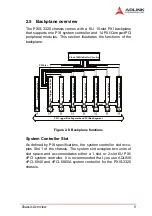


Chassis Overview
11
10 MHz Reference Clock
The backplane supplies every peripheral slot with a 10 MHz sys-
tem clock signal (PXI_CLK10). An independent clock buffer (hav-
ing source impedance matched to the backplane and a skew of
<1ns between slots) drives the clock signals to each peripheral
slot.
You can use this common reference clock signal to synchronize
multiple modules in a measurement or control system or drive
PXI_CLK10 from an external source through the PXI_CLK10_IN
pin on the P2 connector of the star trigger slot.
Содержание PXIS-3320
Страница 4: ......
Страница 12: ...4 Introduction...
Страница 20: ...12 Chassis Overview...
Страница 32: ...24 Specifications...
Страница 34: ...26 Backplane Drawing and Pin Assignments Figure B 2 CBX 6015 rear view...
Страница 46: ...38 Backplane Drawing and Pin Assignments...


