


ADLINK Technology Inc.
LEC-
iMX6R2 User’s Guide
Page 28
copyright © 2021 ADLINK Technology Inc.
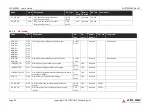
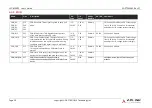
4.3.3
MIPI Camera support
4.3.3.1
MIPI CSI0
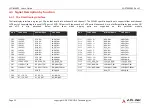
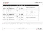
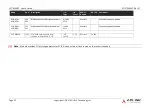
Name
Pin
#
Description
I/O
Type
I/O
Level
Power
Domain
PU / PD
Comments
C
CSI0_RX0-
C
CSI0_RX1-
S11
S12
S14
S15
CSI0 differential input (point to point)
I LVDS D-PHY
/ I LVDS M-PHY
Runtime
CSI0_CK-
S8
S9
CSI0 differential clock intput (point to
point)
I LVDS D-PHY
Runtime
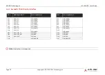
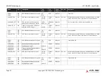
I2C_CAM0_DAT
/ CSI0_TX-
S7
I2C data for serial camera data
support link or differential data lane
I/O OD CMOS
/ O LVDS M-
PHY
1.8V
Runtime
PU 2.2K
MIPI-CSI 2.0 uses I2C_CAM0_DAT
MIPI-CSI 3.0 uses CSI0_TX-
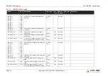
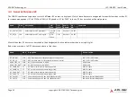
I2C_CAM0_CK /
S5
I2C clock for serial camera data
support link or differential data lane
O OD CMOS
/ O LVDS M-
PHY
1.8V
Runtime
PU 2.2K
MIPI-CSI 2.0 uses I2C_CAM0_CK
MIPI-CSI 3.0 uses
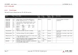
CAM0_PWR# /
GPIO0
P108 Camera 0 Power Enable, active low
output.
O CMOS
1.8V
Runtime
CAM0_RST# /
GPIO2
P110 Camera 0 reset, active low output
O CMOS
1.8V
Runtime
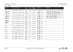
CAM_MCK
S6
Master clock output
O CMOS
1.8V
Runtime
This signal is used by both CSI0 and CSI1
Содержание LEC-IMX6R2
Страница 1: ...LEC IMX6R2 02 12 2021...
Страница 31: ...LEC iMX6R2 User s Guide SGET SMARC Rev 2 1 Page 31 copyright 2021 ADLINK Technology Inc 4 3 5 USB ports...
Страница 62: ...ADLINK Technology Inc LEC iMX6R2 User s Guide Page 62 copyright 2021 ADLINK Technology Inc 6 Mechanical...
Страница 65: ...LEC iMX6R2 User s Guide SGET SMARC Rev 2 1 Page 65 copyright 2021 ADLINK Technology Inc...


