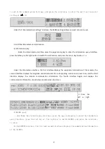
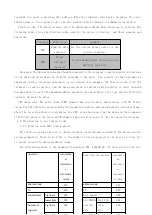
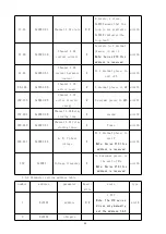
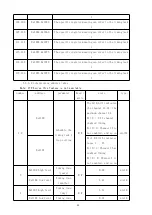
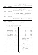

31
1
103-106
0x1066-0x1069
The specific register meaning can refer to the timing task
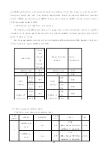
1
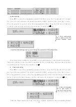
107-110
0x106A-0x106D
The specific register meaning can refer to the timing task
1
111-114
0x106E-0x1071
The specific register meaning can refer to the timing task
1
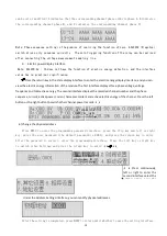
115-118
0x1072-0x1075
The specific register meaning can refer to the timing task
1
119-122
0x1076-0x1079
The specific register meaning can refer to the timing task
1
123-126
0x107A-0x107D
The specific register meaning can refer to the timing task
1
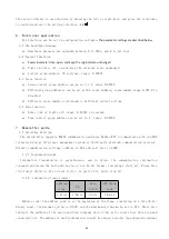
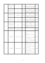
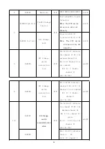
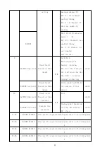
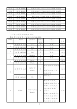
7.3.3.2 Scheduliming address table
Note: 210 Series this feature is not available
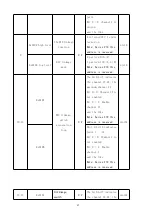
number
address
parameter
Read /
write
scale
type
1-2
0x1100
Schedule the
timing task 1
loop setting
R/W
The bit0-bit7 indicates
the channel 17-24; the
maximum channel 24
Bit 0 = 1:17 channel
enabled timing
Bit 0 = 0: Channel 17 is
not enabled, and so on
uint32
0x1101
Blot 0-bit15 indicates
lanes 1 – 16
Bit 0 = 1: Channel 1 has
enabled timing
Bit 0 = 0: Channel 1 is
not enabled, and so on
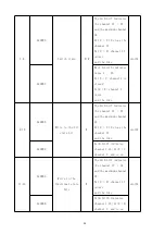
3
0x1102 high level
Timing time
(years)
R/W
0-99
uint8
0x1102 low level
Timing time
(months)
1-12
uint8
4
0x1103 high level
Timing time
(day)
R/W
1-31
uint8
0x1103 low level
Timing time
0-23
uint8