background image

PCIe Accelerator-6D Card User Guide (UG074)

2

www.achronix.com

Speedster FPGAs

Copyrights, Trademarks and Disclaimers

Copyright © 2017 Achronix Semiconductor Corporation. All rights reserved. Achronix, Speedcore, Speedster, 
and ACE are trademarks of Achronix Semiconductor Corporation in the U.S. and/or other countries All other 
trademarks are the property of their respective owners. All specifications subject to change without notice.

NOTICE of DISCLAIMER: The information given in this document is believed to be accurate and reliable. 
However, Achronix Semiconductor Corporation does not give any representations or warranties as to the 
completeness or accuracy of such information and shall have no liability for the use of the information contained 
herein. Achronix Semiconductor Corporation reserves the right to make changes to this document and the 
information contained herein at any time and without notice. All Achronix trademarks, registered trademarks, 
disclaimers and patents are listed at http://www.achronix.com/legal.

Achronix Semiconductor Corporation

2953 Bunker Hill Lane, Suite 101
Santa Clara, CA 95054
USA

Phone : 855.GHZ.FPGA (855.449.3742)
E-mail : [email protected]

Содержание PCIe Accelerator-6D Card

Страница 1: ...Speedster FPGAs www achronix com 1 PCIe Accelerator 6D Card User Guide UG074 Speedster FPGAs ...

Страница 2: ...ment is believed to be accurate and reliable However Achronix Semiconductor Corporation does not give any representations or warranties as to the completeness or accuracy of such information and shall have no liability for the use of the information contained herein Achronix Semiconductor Corporation reserves the right to make changes to this document and the information contained herein at any ti...

Страница 3: ... 10 On Board Memory 11 On Board Temperature Sensor 12 Board Specific Design Issues 12 Chapter 3 Development Environment Setup 13 Installing Achronix Software ACE plus Synopsys Synplify Pro and Licenses 13 Running ACE 13 Setting up the PCIe Accelerator 6D Board 13 Standalone Mode 13 In system Mode 15 Getting started 16 Power Sequencing 16 Initialization 16 Downloading a Design 16 Configuring the Bo...

Страница 4: ...O DIMM Sockets J10 J11 J12 J13 J14 J15 J16 J17 J18 J19 J20 J21 25 User Interfaces 26 FTDI CLI 27 Bitporter CLI 27 ACE GUI 27 SMP Connectors 29 LEDs 30 Switches 31 Miscellaneous Interfaces 31 Chapter 5 PCIe Accelerator 6D Card Clocking 33 Chapter 6 Board Power Supplies 34 Chapter 7 Miscellaneous Diagrams and Figures 36 Revision History 37 ...

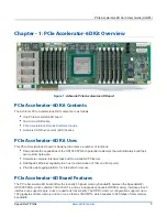
Страница 5: ...00 FPGA to potential customers that will ultimately build their own custom hardware Accelerate compute intensive tasks within a standard PC server Add Gigabit Ethernet capability to a host a combination of 10G and 40G ports Provide a debugging platform for internal Achronix use PCIe Accelerator 6D Board Features The PCIe Accelerator 6D board offers the industry s highest memory bandwidth between t...

Страница 6: ...programmable LUTs hard IP 86 Mb of on chip memory 82 Mb BRAM 4 Mb LRAM 756 28 28 multiply accumulate blocks 960 programmable user I O Network and Communications Hard Ethernet MACs 100GE 40GE 10GE 64 SerDes lanes 1 to 12 75 Gbps Hard Interlaken ports each running up to 11 3 Gbps System Hard PCI Express Gen1 2 3 1 4 8 Hard DDR3 controllers six 72 at 1600 MT s Board PCI Express pluggable form factor ...

Страница 7: ... 6D Board component or device markings Board schematics can be made available upon signing an NDA with Achronix Achronix CAD Environment ACE Software Achronix provides ACE software together with an Achronix optimized version of Synplify Pro from Synopsys a node locked or floating version of the license is needed to use the ACE software for development See PCIe for more details about installation a...

Страница 8: ...PCIe Accelerator 6D Card User Guide UG074 8 www achronix com Speedster FPGAs Save ...

Страница 9: ...ure 3 PCIe Accelerator 6D Board Details User Modes There are two use modes for this development board standalone and in system plug in In both modes the user must provide power to the board through the dedicated power connectors using an external power supply as shown in the figure below Standalone Mode In this mode the development board is placed on a bench with control and data signals coming fr...

Страница 10: ...ode In system Plug in Mode The PCIe Accelerator 6D board is inserted into a PCIe Gen3 8 slot of a PC In addition to the capabilities highlighted in the standalone mode data traffic can be supplied over the PCIe interface in this mode assuming the PCIe interface of the FPGA is configured appropriately This mode is shown in the figure below ...

Страница 11: ...the board On Board Memory The development board has the following memories available for system design Twelve 204 pin DDR3 SO DIMM connectors to allow for loading of 12 DDR3 SO DIMMs each of which has a performance of 12 8 Gbps or 1600 MT s This memory serves as the primary off chip memory for all applications supplementing the on chip BRAM This memory also demonstrates the embedded DDR3 controlle...

Страница 12: ...HD1000 FPGA 2 Board Specific Design Issues The PCIe Accelerator 6D board is optimized for networking and compute acceleration applications As such Achronix has configured the SerDes and the I O at specific pins on the HD1000 device This configuration must maintain during any changes made to the design hosted in the FGPA Achronix provides a template for ACE to avoid inadvertent changes to the confi...

Страница 13: ...g Windows license server Linux node locked Linux client software Windows node locked Windows client software Install licenses e mailed by Achronix on the license server Modify the license servers for floating licenses only cases b c e and f Run the license servers not needed for case a Windows node locked Set the client machine environment variables Run the software For more details on Steps 1 thr...

Страница 14: ...1000 s internal 6D Board Details see page 9 registers via FTDI over JTAG Connect the second supplied micro USB cable to the DCC Micro USB Connector see figure PCIe for accessing the HD1000 s internal registers via DCC Accelerator 6D Board Details see page 9 Connect the extended Gen3 8 PCIe connector to the PCIe edge connector on the board see figure PCIe Accelerator 6D Board Details see page 9 Con...

Страница 15: ...date the clearance requirements for the component side of the board Figure shows the connections for this mode In System Board Connections see page 15 Figure 7 In System Board Connections Connecting the Power Supply Although the individual components on the board use different voltage levels each of these is generated on the board using a single 12V power supply input A spare 12V supply connector ...

Страница 16: ...the board can be controlled via the I C bus by either the 2 on board HD1000 FPGA or through an external device via the DC1613A I C programming connector either of 2 which can act as the I C bus master After power up and initialization the HD1000 becomes the default I C bus 2 2 master Downloading a Design Typically the following steps are needed to download a design to the board and start debugging...

Страница 17: ...ils see page 9 connect the Bitporter pod using the ribbon cable to the JTAG Header see figure Via Bitporter PCIe Connect the USB end of Bitporter pod to USB port of the Accelerator 6D Board Details see page 9 host PC Power up the board Run ACE and switch to Programming and Debug Perspective or HW Demo Perspective to program the bitstream Once the FPGA is programmed and the CONFIG_DONE LED light is...

Страница 18: ...on the HD1000 FPGA and the Accelerator 6D board These interfaces are discussed in more detail in the following sections Networking and Communications Interface see page 19 System Interfaces see page 22 Memory Interface see page 25 User Interfaces see page 26 Miscellaneous Interfaces see page 31 Figure 8 PCIe Accelerator 6D Card Interfaces ...

Страница 19: ...0G 4 QSFP transceiver modules 16 10G with split out cables The four port QSFP cage is directly connected to 16 bidirectional 12 5 G SerDes lanes These are designated in quads as SerDes CH0 8 11 CH1 16 19 CH2 24 27 CH3 28 31 as shown in the figure above Table below shows the pin assignment for the QSFP interface to the HD1000 SerDes pin Table 2 Accelerator 6D Rev C QSFP Interface Pins QSFP Module P...

Страница 20: ...ID_TX1_P B27 R_MID_TX2_N B28 R_MID_TX2_P A28 R_MID_TX3_N C29 R_MID_TX3_P B29 R_MID_TX4_N B30 R_MID_TX4_P A30 R_MID_RX1_N E27 R_MID_RX1_P F27 R_MID_RX2_N F28 R_MID_RX2_P G28 R_MID_RX3_N E29 R_MID_RX3_P F29 R_MID_RX4_N F30 R_MID_RX4_P G30 L_MID_TX1_N CH 2 24 27 C35 L_MID_TX1_P B35 L_MID_TX2_N B36 L_MID_TX2_P A36 L_MID_TX3_N C37 L_MID_TX3_P B37 L_MID_TX4_N B38 L_MID_TX4_P A38 ...

Страница 21: ... E35 L_MID_RX1_P F35 L_MID_RX2_N F36 L_MID_RX2_P G36 L_MID_RX3_N E37 L_MID_RX3_P F37 L_MID_RX4_N F38 L_MID_RX4_P G38 LEFT_TX1_N CH 3 28 31 C39 LEFT_TX1_P B39 LEFT_TX2_N B40 LEFT_TX2_P A40 LEFT_TX3_N C41 LEFT_TX3_P B41 LEFT_TX4_N B42 LEFT_TX4_P A42 LEFT_RX1_N E39 LEFT_RX1_P F39 LEFT_RX2_N F40 LEFT_RX2_P G40 LEFT_RX3_N E41 LEFT_RX3_P F41 LEFT_RX4_N F42 LEFT_RX4_P G42 ...

Страница 22: ... above shows the dedicated PCIe pins on the HD1000 designated SerDes Bottom 0 7 in the figure The table below shows the pins on the HD1000 and their connections to the PCIe edge connector Note Power is not supplied to the board via the PCIe connector Table 3 HD1000 PCIe Edge Connector Mapping Signal Name SerDes No Pin on HD1000 U1 Pin on PCIe 8 Finger J2 PCIE0_PERST_N_LT P15 A11 via U33 PCIE0_RX0_...

Страница 23: ...B15 A29 PCIE0_TX3_N C15 A30 PCIE0_RX4_P 4 G14 B33 PCIE0_RX4_N F14 B34 PCIE0_TX4_P A14 A35 PCIE0_TX4_N B14 A36 PCIE0_RX5_P 5 F13 B37 PCIE0_RX5_N E13 B38 PCIE0_TX5_P B13 A39 PCIE0_TX5_N C13 A40 PCIE0_RX6_P 6 G12 B41 PCIE0_RX6_N F12 B42 PCIE0_TX6_P A12 A43 PCIE0_TX6_N B12 A44 PCIE0_RX7_P 7 F11 B45 PCIE0_RX7_N E11 B46 PCIE0_TX7_P B11 A47 PCIE0_TX7_N C11 A48 SERDES_BOT_REFCLK_0_P M25 A13 M26 J25 J26 ...

Страница 24: ... FT232RL REEL Table 4 Accelerator 6D Rev C USB J7 Interface Connections HD1000 U1 USB Connector U54 Auxiliary UART U19 HD1000 U1 Signal Name Pin Signal Name Pin Signal Name Pin D 3 USB_D_P 15 FPGA_UART_TX AC42 D 2 USB_D_N 16 FPGA_UART_RX AC43 The second USB J8 port is used for programming the bitstream and communicating with HD1000 via a USB to multipurpose UART FTDI device U54 FPGA bitstream prog...

Страница 25: ...Interface SO DIMM Sockets J10 J11 J12 J13 J14 J15 J16 J17 J18 J19 J20 J21 The Accelerator 6D board has twelve standard 204 pin DDR3 72 bit ECC SO DIMM sockets J10 through J21 with two per each of the six available DDR3 hard IP controllers on the HD1000 FPGA These SODIMM sockets can be used to load 12 DDR3 ECC SODIMMs of up to 16 GB each to give a total of 192 gigabytes of on board memory With the ...

Страница 26: ...gle rank single slot Dual rank single slot Dual rank dual slot User Interfaces The following interfaces can be used to configure and drive the board connect cables review status of the board and perform other functions related to development work FTDI CLI see page 27 Bitporter CLI see page 27 ACE GUI see page 27 SMP Connectors see page 29 LEDs see page 30 Switches see page 31 ...

Страница 27: ...xe line interface CLI window on the development PC to download and configure the HD1000 For more details on programming the HD1000 FPGA using the Achronix STAPL Player refer to the Bitstream Programming and Chapter 4 Using the Achronix STAPL Player Debug Interface User Guide Note Care must be taken when powering up the Bitporter pod and the development board Refer to the for more details Bitstream...

Страница 28: ...PCIe Accelerator 6D Card User Guide UG074 28 www achronix com Speedster FPGAs Figure 10 ACE GUI for Bitstream Programming Figure 11 ACE GUI for Register Access via JTAG ...

Страница 29: ...PCIe Accelerator 6D Card User Guide UG074 Speedster FPGAs www achronix com 29 Figure 12 ACE GUI for Real time Design Debug Figure 13 ACE GUI for Hardware Demo SMP Connectors ...

Страница 30: ...3002 Single ended FPGA external clock LEDs There are eleven LEDs on the board Three are dedicated to provide status information while the rest are user programmable The following table lists all the LEDs their function and connection to HD1000 FPGA Table 8 LED Connections LED Function Net Name Component Pin DS3000 Board Power Good indicator POWR_GOOD_3V3 U3014 F6 DS3001 Configuration status indica...

Страница 31: ...choose between programming the HD1000 FPGA via JTAG or SPI Miscellaneous Interfaces The PCIe Accelerator 6D board has a Linear DC1613A USB to I C pod connector interface which is a 12 pin I C 2 2 header J3 that allows for communication over the I C bus to all the various devices on the board With this 2 interface the DC1613A pod can control monitor various voltages power and current of all the pow...

Страница 32: ...PCIe Accelerator 6D Card User Guide UG074 32 www achronix com Speedster FPGAs Pin Net Name Pin 8 Pin 9 Pin 10 GND Pin 11 Pin 12 ...

Страница 33: ...uired to implement the system level functions For more details on HD1000 clock bank PLLs and clocking architecture refer to the Speedster22i Clock and Reset Networks User Guide UG027 Three 156 26 MHz 3 3V LVPECL differential clocks provide the SerDes PMA reference clocks to HD1000 s bottom four groups of four SerDes lanes each bottom SerDes CH0 8 11 CH1 16 19 CH2 24 27 CH3 28 31 These connect to t...

Страница 34: ...CC_3V3 LTM4633 U34 5 3 3 VCC_1V8 LTM4633 U34 5 1 8 VCC0V95 LTM4633 U34 5 0 95 VCC_1V0_3 VDDA_NOM_E LT3083 U3002 1 5 1 VCC_1V0_4 VDDA_NOM_W LT3083 U3003 1 5 1 VCC_1V7 LT3022 U91 3 3 1 7 FPGA_VREF LT3020 U92 1 0 762 DDR3 SODIMM EC Slot 1 J13 Slot 0 J12 DDR_EC_VREF VTT LTC3617 U5 5 0 75 DDR3 SODIMM EN Slot 1 J11 Slot 0 J10 DDR_EN_VREF VTT LTC3617 U4 5 0 75 DDR3 SODIMM ES Slot 1 J15 Slot 0 J14 DDR_ES_...

Страница 35: ...eedster FPGAs www achronix com 35 Component Component Number Power Rail Power Regulator Component Number VIN V VOUT V DDR3 SODIMM WS Slot 1 J20 Slot 0 J21 DDR_WS_VREF VTT LTC3617 U3 5 0 75 Heatsink Fan Header J9 Heatsink Fan F 5010HH12B III 12 NA ...

Страница 36: ...erator 6D Card User Guide UG074 36 www achronix com Speedster FPGAs Appendix Miscellaneous Diagrams and Figures Figure Note I C Address is 7 bits plus a read write bit 2 Figure 15 Board Device Power and I C Map 2 ...

Страница 37: ... achronix com 37 Revision History Version Date Description 1 0 March 20 2017 Initial Achronix release 1 1 March 23 2017 Added table to the I C Header J3 Pin Connections 2 see page 31 Mis section cellaneous Interfaces see page 31 Fixed broken reference links Save ...

Отзывы: