background image

Manual PCI-DIO-48JP/JPS 

14


Bit Assignment 

Code 

D0 
D1 
D2 
D3 
D4 

D5,D6 

D7 

Port C Lo (C0-C3) 
Port B 
Mode Select 
Port C Hi (C4-C7) 
Port A 
Mode Select 
Mode Set Flag 

1=Input, 0=Output 
1=Input, 0=Output 
1=Mode 1, 0=Mode 0 
1=Input, 0=Output 
1=Input, 0=Output 
00=Mode 0, 01=Mode 1, 1X=Mode 2 
1=Active 


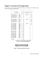
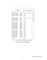
Table 6-2: Control Register Bit Assignment 

  
Note: 

Mode 1 cannot be used by these cards without modification. Thus, bits D2, D5, and D6 
should always be set to "0". If your card has been modified to operate in Mode 1, then there 
will be an Addendum page in the front of this manual. These cards cannot be used in Mode 
2 of the PPI. 

 
These cards provide a means to enable/disable the tristate I/O buffers under program control. If the 
TST/BEN jumper on the card is installed in the BEN position, the I/O buffers are permanently enabled. 
However, if that jumper is in the TST position, enable/disable of the buffers is 

software controlled

 via the 

control register as follows: 

  
a. The card is initialized in the receive mode by the computer reset command. 
  
b. When bit D7 of the Control Register is set high, direction of the three groups of the associated PPI 
chip as well as the mode can be set. For example, a write to Base A3 with data bit D7 high 
programs port direction at group 0 ports A, B, and C. If, for example, hex 80 is sent to Base Address 
+3, the group 0 PPI will be configured in mode 0 with ports A, B, and C as outputs. 
  
At the same time, data bit D7 is also latched in a buffer controller for the associated PPI chip. A high 
state disables the buffers and, thus, all four buffers will be put in the tristate mode; i.e. disabled. 
  
c. If any of the ports are to be set as outputs, you may set the values to the respective port with the 
outputs still in the tristate condition. (If all ports are to be set as inputs, this step is not necessary.) 
  
d. If data bit D7 is low when the control byte is written, ONLY the associated buffer controller is 
addressed. If, for example, a control byte of hex 80 has been sent as previously described, and the 
data to be output are correct, and it is now desired to open the three ports, then it is necessary to send 
a control byte of hex 00 to base a3 to enable the port 0 buffers. When you do this, the buffers 
will be enabled. 
 

Note that all data bits except D7 must be the same for the two control bytes 
 
Those buffers will now remain enabled until another control byte with data bit D7 high is sent to base 
a3. 
 

Содержание PCI-DIO-48S

Страница 1: ...3 Roselle Street San Diego CA 92121 858 550 9559 FAX 858 550 7322 contactus accesio com www accesio com DIGITAL INPUT OUTPUT CARD Models PCI DIO 48JP and PCI DIO 48JPS USER MANUAL File MPCI DIO 48JPS...

Страница 2: ...CES nor the rights of others IBM PC PC XT and PC AT are registered trademarks of the International Business Machines Corporation Printed in USA Copyright 1998 2005 by ACCES I O Products Inc 10623 Rose...

Страница 3: ...or parts not excluded by warranty Warranty commences with equipment shipment Following Years Throughout your equipment s lifetime ACCES stands ready to provide on site or in plant service at reasonabl...

Страница 4: ...ss Selection 10 Chapter 5 Software 11 Chapter 6 Programming 13 Table 6 1 Address Assignment Table 13 Table 6 2 Control Register Bit Assignment 14 Table 6 3 Control Register Configuration 15 Table 6 4...

Страница 5: ...interface to 48 lines Each PPI provides three 8 bit ports A B and C Each 8 bit port can be software configured to function either as inputs or as latched outputs Port C can also be software configured...

Страница 6: ...ddress space The base address is selected by the system An illustrated setup program is provided on the diskette or CD shipped with your card Interactive displays show locations and proper configurati...

Страница 7: ...ns for usage of the various card options CD Software Installation The following instructions assume the CD ROM drive is drive D Please substitute the appropriate drive letter for your system as necess...

Страница 8: ...ned resources 10 Run one of the provided sample programs that was copied to the newly created card directory from the CD to test and validate your installation The base address assigned by BIOS or the...

Страница 9: ...ng or disabling the 74LS245 input output buffers under program control is provided at the jumper position labeled TST BEN When the jumper is in the BEN Buffer Enable position the I O buffers are alway...

Страница 10: ...of the cards and the respective IRQs allotted Alternatively some operating systems Windows95 and WindowsNT 5 0 can be queried to determine which resources were assigned In these operating systems you...

Страница 11: ...ions are in the form of a DLL a GBL and a VisualBASIC sample Together these files allow you to access the port and main memory space in a fashion similar to BASIC QuickBASIC Pascal C C Assembly and mo...

Страница 12: ...t less intuitive All integers in BASIC are signed numbers wherein data are stored in two s complement form All bit patterns must be converted to and from this two s complement form if meaningful displ...

Страница 13: ...0 Port C Group 0 Control Group 0 Port A Group 1 Port B Group 1 Port C Group 1 Control Group 1 Enable Disable Buffer Grp 0 Enable Disable Buffer Grp 1 Enable Chg of St Interrupt Clear Chg of St Interru...

Страница 14: ...sociated PPI chip as well as the mode can be set For example a write to Base Address 3 with data bit D7 high programs port direction at group 0 ports A B and C If for example hex 80 is sent to Base Ad...

Страница 15: ...ow See item d above outportb BASE_ADDRESS 3 0x09 PROGRAMMING EXAMPLE BASIC The following example in BASIC is provided as a guide to assist you in developing your working software In this example the c...

Страница 16: ...ite to the Control Register with bit D7 low If you wish to subsequently disable the buffers you can write to the Control Register with bit D7 high In this way you can enable disable the output buffers...

Страница 17: ...dress Bh Toggle bit C3 high for at least 1 uS then low Note that this pulse will show up at pin 5 or 41 of the connector Example 2 External interrupt The interrupt option jumper for the group must be...

Страница 18: ...0 Port B Group 0 Port B Group 0 Port B Group 0 Port B Group 0 Port B Group 0 Port B Group 0 Port B Group 0 Port B Group 0 Port A Group 0 Port A Group 0 Port A Group 0 Port A Group 0 Port A Group 0 Po...

Страница 19: ...rt B Group 1 Port B Group 1 Port B Group 1 Port B Group 1 Port A Group 1 Port A Group 1 Port A Group 1 Port A Group 1 Port A Group 1 Port A Group 1 Port A Group 1 Port A 5 VDC PC7 PC6 PC5 PC4 PC3 PC2...

Страница 20: ...manual or just want to give us some feedback please email us at manuals accesio com Please detail any errors you find and include your mailing address so that we can send you any manual updates 10623...

Отзывы: