Appendix
A96G140/A96G148/A96A148 User’s manual
258
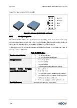
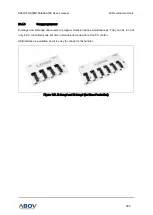
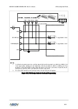
Figure 135 shows pinouts of OCD connector.
Figure 135. Debugger (OCD1/OCD2) and Pinouts
20.3.1
On-chip debug system
The A96G140/A96G148/A96A148 supports On-chip Debug (OCD) system. We recommend developing
and debugging program with A96G1xx series. The OCD system of the A96G140/A96G148/A96A148
can be used for programming the non-volatile memories and on-chip debugging.
In this section, you can find detailed descriptions for programming via the OCD interface. Table 57
introduces features of the OCD.
Table 57. OCD Features
Two wire external interface
1 for serial clock input
1 for bi-directional serial data bus
Debugger accesses
All internal peripherals
Internal data RAM
Program Counter
Flash memory and data EEPROM memory
Extensive
On-Chip
Debugging
supports for Break Conditions
Break instruction
Single step break
Program memory break points on single address
Programming of Flash, EEPROM, Fuses, and Lock
bits through the two-wire interface
On-Chip Debugging supported by Dr. Choice
Operating frequency
The maximum frequency of a target MCU.
2 User VCC
1
3
4
5
6
7
8
10
9
User GND
DSCL
DSDA


