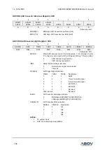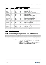
15. USI
A96G140/A96G148/A96A148 User’s manual
170
In master mode of operation, even if transmission is not enabled (TXEn=0), writing data to the USInDR
register is necessary because the clock SCKn is generated from transmitter block.
15.12
USIn SPI block diagram
RXCIEn
Rx Control
Receive Shift Register
(RXSR)
Data
Recovery
DORn Checker
USInDR[0], (Rx)
Tx Control
Transmit Shift Register
(TXSR)
USInDR, (Tx)
I
N
T
E
R
N
A
L
B
U
S
L
I
N
E
M
U
X
LOOPSn
TXCn
TXCIEn
DRIEn
DREn
Empty signal
To interrupt
block
INT_ACK
Clear
RXCn
Baud Rate Generator
USInBD
TXEn
SCLK
(fx: System clock)
MISOn
MOSIn
M
U
X
MASTERn
D
E
P
FXCHn
SCKn
SCK
Control
MASTERn
RXEn
To interrupt
block
M
U
X
Edge Detector
And
Controller
SSn
SS
Control
CPHAn
CPOLn
ORDn
(MSB/LSB-1st)
USInDR[1], (Rx)
USInSSEN
Figure 93. USIn SPI Block Diagram (n = 0 and 1)
15.13
USIn I2C mode
The USIn can be set to operate in industrial standard serial communication protocols mode. The I2C
mode uses 2 bus lines serial data line (SDAn) and serial clock line (SCLn) to exchange data. Because
both SDAn and SCLn lines are open-drain output, each line needs pull-up resistor. The features are as
shown below.
Compatible with I2C bus standard
Multi-master operation
Up to 400kHz data transfer read speed
7 bit address


