BIOS Setup
3-7
3.3. Advanced Chipset Features
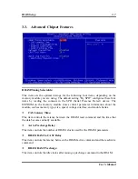
DRAM Timing Selectable:
This item sets the optimal timings for the following four items, depending on the
memory module you are using. The default setting “By SPD” configures these four
items by reading the contents in the SPD (Serial Presence Detect) device. The
EEPROM on the memory module stores critical parameter information about the
module, such as memory type, size, speed, voltage interface, and module banks.
CAS Latency Time:
This item controls the latency between the DRAM read command and the time that
the data becomes actually available.
Act to Precharge Delay:
This item controls the number of DRAM clocks used for the DRAM parameters.
DRAM RAS# to CAS# Delay
This item controls the latency between the DRAM active command and the read/write
command.
DRAM RAS# Precharge:
This item controls the idle clocks after issuing a precharge command to the DRAM.
User’s Manual
Содержание SI-1Ns42
Страница 1: ...SI 1Ns42 SI 1Ns60 Intel Pentium 4 Server Board Socket 478 User s Manual Rev 1 00...
Страница 7: ...Introduction 1 3 1 2 Layout User s Manual...
Страница 25: ...Hardware Setup 2 17 2 17 Low Pin Count Connection Header Reserved for internal testing User s Manual...
Страница 35: ...BIOS Setup 3 9 3 4 Integrated Peripherals OnChip IDE Device Click Enter key to enter its submenu User s Manual...
Страница 48: ...3 22 Chapter 3 3 22 Chapter 3 SI 1Ns42 SI 1Ns60 SI 1Ns42 SI 1Ns60...


