YUGE CLM920 NC2 LTE M.2, Hardware Usage Manual
The YUGE CLM920 NC2 LTE M.2 is a high-performance hardware device that requires a Hardware Usage Manual for proper setup and maintenance. You can download the manual for free from manualshive.com to optimize the functionality of this product. Stay informed and get the most out of your investment.
Share
Download


Reviews:
No comments
Related manuals for CLM920 NC2 LTE M.2
p600 Series
Brand: Acer Pages: 44
p600 Series
Brand: Acer Pages: 44
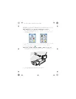
e300 Series
Brand: Acer Pages: 2

Pathfinder
Brand: Raymarine Pages: 111

DPN-3500
Brand: Daewoo Pages: 62

TR-11E
Brand: C2STek Pages: 8
Tracker 5380
Brand: Navman Pages: 64

GT-1800A
Brand: I-gotU Pages: 2

40 Easy
Brand: Navigon Pages: 125
Vulcan Series
Brand: B&G Pages: 68

nuvi 3597LMTHD
Brand: Garmin Pages: 22

nuvi 5000
Brand: Garmin Pages: 12

Quest TM
Brand: Garmin Pages: 68

AATDriver
Brand: MyFlyDream Pages: 7

HI-406BT
Brand: Clas Ohlson Pages: 36

eXplorist 510
Brand: Magellan Pages: 51

CelloTrack T
Brand: Cellocator Pages: 20
GPS103-A
Brand: Coban Pages: 19


