SERVICE MANUAL
Sony Corporation
Audio&Video Business Group
Published by Sony Techno Create Corporation
ICD-UX71/UX71F/UX81/
UX81F/UX91F
SPECIFICATIONS
IC RECORDER
9-889-311-01
2008J04-1
©
2008.10
AEP Model
ICD-UX71/UX71F/UX81/UX81F
E Model
Chinese Model
ICD-UX71F/UX81F/UX91F
Latin American Model
ICD-UX71/UX71F/UX81/UX81F
Ver. 1.0 2008.10
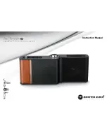
Photo: ICD-UX71
IC recorder section
Capacity (User available capacity)
ICD-UX71/UX71F:
1 GB (approx. 986 MB =1,034,354,688 Byte)
ICD-UX81/UX81F:
2 GB (approx. 1.92 GB =2,072,313,856 Byte)
ICD-UX91F:
4 GB (approx. 3.86 GB =4,147,806,208 Byte)
A part of the memory capacity is used as a
management area.
Recording time
*
1
ICD-UX71/UX71F
ST mode
STSP mode
STLP mode
11 hr. 55 min. 17 hr. 55 min. 47 hr. 50 min.
SP mode
LP mode
71 hr. 45 min. 287 hr. 15 min.
ICD-UX81/UX81F
ST mode
STSP mode
STLP mode
23 hr. 55 min. 35 hr. 55 min. 95 hr. 55 min.
SP mode
LP mode
143 hr. 50 min. 575 hr. 35 min.
ICD-UX91F
ST mode
STSP mode
STLP mode
47 hr. 55 min. 72 hr.
192 hr.
SP mode
LP mode
288 hr.
1152 hr. 5 min.
(hr. : hours/min. : minutes)
*
1
When you are going to record continuously
for a long time, you may have to replace
the battery with a new one in the midst of
recording.
Frequency range
z
ST : 40 Hz - 20,000 Hz
z
STSP : 40 Hz - 15,000 Hz
z
STLP : 60 Hz - 7,500 Hz
z
SP : 60 Hz - 10,000 Hz
z
LP : 60 Hz - 3,400 Hz
Bit rates and sampling frequencies for
MP3
fi
les
*
2
Bit rate: 32 - 320 kbps, VBR
Sampling frequencies: 16/22.05/24/32/44.1/
48 kHz
*
2
The playback of MP3
fi
les recorded using the
IC recorder is also supported.
Not all encoders are supported.
Bit rate and sampling frequencies
*
3
for
WMA
fi
les
Bit rate: 32 - 192 kbps*
4
, VBR
Sampling frequencies: 44.1 kHz
*
3
WMA Ver. 8 Class2A is compatible, however,
MBR (Multi Bit Rate), Lossless, Professional,
and Voice are not supported.
*
4
The NoiseSubstitution function is not
supported, therefore, playback becomes
simple playback with 32 kbps bit rate.
FM radio section
Frequency range
87.5 - 108 MHz
IF 150 kHz
Antenna
Headphone cord antenna
General
Speaker
Approx. 10 mm dia.
Power output
90 mW
Input/Output
z
Microphone jack (minijack, stereo)
– input for plug in power, minimum input
level 0.9 mV, 3 kilohms or lower impedance
microphone
z
Headphone jack (minijack, stereo)
– output for 8 - 300 ohms headphones
z
USB connector
– High-Speed USB compatible
Playback speed control (DPC)
+100% to –50% (MP3)
0% to –50% (WMA)
Power requirements
One NH-AAA rechargeable battery (supplied):
1.2 V DC
One LR03 (size AAA) alkaline battery (not
supplied): 1.5 V DC
Operating temperature
5
˚
C - 35
˚
C
– Continued on next page –