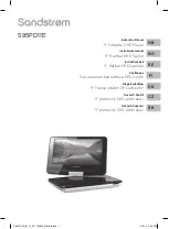
background image

FILE .NO

VCD-X220

Service Manual

Portable VCD/CD Player

PRODUCT CODE No.

Specifications

1 164 160 00   VCD-X220 (SS)

REFERENCE No. SM3600000

System

Laser diode properties

Compact disc digital audio/video system

Material: GaAIAs
Wavelength: 

λ

 = 780nm

Emission duration: Continuous
Laser output: Less than 44.6uW

(This output is the value measured at a distance of 200mm from 
the objective lens surface on the optical pick-up block with 7mm 
aperture.)

D-A conversion

Channel number

Frequency response

Output 
(at 4.5V input level)

Power requirements

1-bit quartz time-axis control

2 channel

20-20,000Hz   

Audio output (stereo mini jack)
Approx. 5mW+ Approx. 5mW at 32 ohms
Video output
Output level 1Vp-p at 75 ohms
Recommended load impedance 75 ohms

Two AA batteries: 3V DC
AC power adapter (DC IN 4.5V jack):
110 or 220V 50/60Hz Switchable.

Battery life
(approx. Hours) 

(When you use the VIDEO CD player on a flat 
and stable surface.)
Player time varies depending on how the CD 
player is used.

VCD

3

2.0

1.5

MP3

CD

5.5

4.5

4.5

Two
NIMH 1800mAh
Batteries

Two
NIMH 1200mAh
Batteries

Two
Alkaline Batteries
LR6

5.5

4

4

Operating temperature

Dimensions (w/h/d)
(excluding projecting 
parts and controls)

Mass

o

o

5 C - 35 C

Approx. 128X26X137mm

Unit Net Weight : 210gr.

Specifications subject to change without notice.

Summary of Contents for VCD-X220

Page 1: ...bit quartz time axis control 2 channel 20 20 000Hz Audio output stereo mini jack Approx 5mW Approx 5mW at 32 ohms Video output Output level 1Vp p at 75 ohms Recommended load impedance 75 ohms Two AAbatteries 3V DC AC power adapter DC IN 4 5V jack 110 or 220V 50 60Hz Switchable Battery life approx Hours When you use the VIDEO CD player on a flat and stable surface Player time varies depending on ho...

Page 2: ...18 19 17 16 S02 S01 10 9 8 4 3 1 2 5 6 7 12 13 14 15 11 1 EXPLODED VIEW ...

Page 3: ...r 22K R15 TG22 61452235 00 Chip Resistor 22K R16 TG22 61452235 00 Chip Resistor 22K R17 TG22 61454735 00 Chip Resistor 47K R18 TG22 61451035 00 Chip Resistor 10K R19 TG22 61451035 00 Chip Resistor 10K R3 TG22 61451015 00 Chip Resistor 100 R4 TG22 61451025 00 Chip Resistor 1K R5 TG22 61451005 00 Chip Resistor 10 R6 TG22 61452235 00 Chip Resistor 22K R7 TG22 61452735 00 Chip Resistor 27K R8 TG22 614...

Page 4: ...2 61452235 00 Chip Resistor 22K R102 TG22 61451035 00 Chip Resistor 10K R103 TG22 61451035 00 Chip Resistor 10K R160 TG22 61454725 00 Chip Resistor 4 7K R302 TG22 61455625 00 Chip Resistor 5 6K R303 TG22 61455625 00 Chip Resistor 5 6K RK1 TG29 28000001 00 Remote Sensor 3 3V SW1 TG18 45110000 00 Detect Switch CD DOOR SW2 TG18 31220000 00 Slide Switch 2P2T SW4 TG18 31220000 00 Slide Switch 2P2T U1 T...

Page 5: ...U5 M11L416256SA SDRAM U6 W27C020P EP ROM U3 LS 188 VCD Decode U2 TZA1024 Optic system Mech Deck U1 BH6575 Motor driver Power control SVCC 3 3V VIDEO OUTPUT U9 SAA7324H M2B DSP and DAC System U12 CS8553 TV ENCODE U8 U10 BA4510 BH4453 POWER AMPLIFIER AUDIO OUTPUT ...

Page 6: ...Pin 21 22 23 24 25 26 27 28 29 START 1 DC DC converter starting terminal OFF 2 DC DC converter OFF terminal CLK 3 External clock synchronization input terminal MUTE34 4 CH3 4 mute terminal MUTE1 5 CH1 mute terminal RESET 6 Reset output terminal IN1 7 CH1 input terminal IN2 8 CH2 input terminal IN3 9 CH3 input terminal IN4 10 CH4 input terminal VREF 11 Reference power supply input terminal DC_IN 30...

Page 7: ...rent output to laser diode VDD L laser supply voltage CFIL external filter capacitor MON laser monitor diode input DIN central diode input GND ground Pin 1 2 3 4 5 6 7 Symbol Description CMFB common mode feedback voltage input RFFB external RF feedback resistor Pin 8 9 RFEQO 10 RF amplifier output CDRW 11 gain select input for CD A V CD R W EQSEL 12 equalizer speed select input n 1 2 or 4 VDD 13 s...

Page 8: ...ance output 7 Pin 36 37 VDAT_6 38 Luminance output 6 VDAT_5 39 Luminance output 5 VDAT_4 40 Luminance output 4 VDAT_3 41 Luminance output 3 VDAT_2 42 Luminance output 2 EMI_A_3 15 EMI Adress Bus Outputs 3 VDD_IO_00 16 System I O power supply EMI_A_4 17 EMI Adress Bus Outputs4 EMI_A_5 18 EMI Adress Bus Outputs 5 VSS_IO_00 19 System I O ground EMI_A_6 20 EMI Adress Bus Outputs 6 EMI_A_7 21 EMI Adres...

Page 9: ...robe output VSS_CORE_20 111 System core ground LRAS_L 112 Lower row address strobe outputs DR_A_8 113 DRAM Address bus outputs 8 DR_A_0 114 DRAM Address bus outputs 0 DR_A_7 115 DRAM Address bus outputs 7 DR_A_1 116 DRAM Address bus outputs 1 DR_A_6 117 DRAM Address bus outputs 6 VSS_IO_30 118 System I O ground DR_A_2 119 DRAM Address bus outputs 2 DR_A_5 120 DRAM Address bus outputs 5 VSS_CORE_30...

Page 10: ...C SCL1 37 serial bit clock input for data loopback to DAC RESET 38 power on reset input active low SDA 39 microcontroller interface data l o line l2c busopen drain output SCL 40 microcontroller interface clock line input l2c bus RAB 41 microcontroller interface R W and load control line input 4 wire bus mode SILD 42 microcontroller interface R W and load control line input 4 wire bus mode STATUS 4...

Page 11: ...ficance P 7 4 25 YCbCr pixel inputs TTL compatible Also synchronized by CLK with respect to the incoming HSYNC timing the higher index corresponds to a greater significance P 7 5 26 YCbCr pixel inputs TTL compatible Also synchronized by CLK with respect to the incoming HSYNC timing the higher index corresponds to a greater significance P 7 6 27 YCbCr pixel inputs TTL compatible Also synchronized b...

Page 12: ...11 WIRING CONNECTION MAIN PCB KEY PCB CD MECHANISM LCD DISPLAY DESCRIPTION ...

Page 13: ...9 1 3 2 1 1 7 3 3 0 PLAY VCD 2 2 2 5 1 1 1 8 1 2 0 2 3 1 2 0 2 9 1 3 2 1 1 7 3 3 0 U4 U5 M11L416256SA SDRAM PIN 1 2 3 4 5 6 7 8 9 10 11 12 13 14 15 3 3 1 7 1 7 1 7 1 7 3 3 1 7 1 7 1 7 1 7 0 0 3 3 3 3 0 PIN 17 18 19 20 21 22 23 24 25 26 27 28 29 30 31 1 3 1 1 3 3 3 0 0 0 0 0 0 0 3 3 3 3 0 1 7 PIN 33 34 35 36 37 38 39 40 1 7 1 7 0 1 7 1 7 1 7 1 7 0 U6 W27C020 EPROM PIN 1 2 3 4 5 6 7 8 9 10 11 12 13 ...

Page 14: ...13 SCHEMATIC DIAGRAM MAIN PCB 1 2 ...

Page 15: ...14 SCHEMATIC DIAGRAM MAIN PCB 1 2 TO KEY PCB ...

Page 16: ...15 SCHEMATIC DIAGRAM MAIN PCB 2 2 ...

Page 17: ...16 SCHEMATIC DIAGRAM MAIN PCB 2 2 ...

Page 18: ...17 CN901 SCHEMATIC DIAGRAM KEY PCB ...

Page 19: ...18 SW2 J2 J3 WIRING DIAGRAM MAIN PCB TOP VIEW ...

Page 20: ...19 WIRING DIAGRAM MAIN PCB BOTTOM VIEW ...

Page 21: ...20 WIRING DIAGRAM KEY PCB TOP VIEW BOTTOM VIEW ...

Page 22: ...SANYO Electric Co Ltd Osaka Japan Mar 03 Printed in China ...

Reviews: