background image


ELECTRONIC CASH REGISTER

C O N T E N T S 

ELECTRONIC CASH REGISTER 

Manual


1.   Precaution Statements 

2.   Product Specifications 

3.   Installation and Operation 

4.   Disassembly and Assembly 

5.   Alignment and Adjustment 

6.   Troubleshooting 

7.      Exploded Views and Parts List 
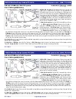
8.   PCB Parts List 

9.   Block Diagram 

10.  Wiring Diagram 

11.  Schematic Diagrams 


SERVICE


ER-350

SERIES 


Summary of Contents for ER-350 II SERIES

Page 1: ... Precaution Statements 2 Product Specifications 3 Installation and Operation 4 Disassembly and Assembly 5 Alignment and Adjustment 6 Troubleshooting 7 Exploded Views and Parts List 8 PCB Parts List 9 Block Diagram 10 Wiring Diagram 11 Schematic Diagrams SERVICE ER 350ⅡSERIES ...

Page 2: ...s Electronic Cash Register Notes Notes may appear anywhere in the manual They describe additional information about the item Precaution symbols Indicates a Safety Precaution that applies to this part component Indicates the part or component is an electro statically sensitive device Use caution when handling these parts ...

Page 3: ...ual may not in whole or in part be copied photocopied reproduced translated or converted to any electronic or machine readable from without prior written permission of Shin Heung Precision SAM4S ER 350Ⅱ Series Service Manual First edition JAN 2006 V1 0 Printed in KOREA ...

Page 4: ...l is subject to change without prior notice Therefore you must check the correspondence of your manual with your machine No part of this manual may be copied or reproduced in any form or by any means without the prior written consent of Shin Heung Precision Note Before using this Electronic Cash Register ECR for the first time leave it powered on in the REG mode for at least twenty four hours This...

Page 5: ...edges and especially the AC and high voltage supplies Always inspect for pinched out of place or frayed wiring Do not change the spacing between comp onents and the printed circuit board Check the AC power cord for damage Make sure that leads and components do not touch thermally hot parts 7 Product Safety Notice Some electrical and mechanical parts have special safety related characteristics whic...

Page 6: ...instrument s ground lead to the instrument chassis ground before connecting the positive lead always remove the instrument s ground lead last 1 3 Precautions for Electrostatic Sensitive Devices ESDs 1 Some semiconductor solid state devices are easily damaged by static electricity Such components are called Electrostatic Sensitive Devices ESDs examples include integrated circuits and some field eff...

Page 7: ...M 310A 9 pin Dot matrix Printing speed 3 2 line per second Specification page 2 2 Processor Winbond W78C438 40 Memory SRAM KM681000 1Mbit EPROM 27C020 2Mbit Data Storage 60 Days When battery fully charged Battery Ni MH 3 6V 70mA Charging time 24 hours Battery backup Display Front 10 digits VFD Rear 10 digits VFD Key Board 44 key or 48 key Raised Interface RS 232C 1 port Drawer 4B 8C 5B 5C 7B 8C We...

Page 8: ...inting Columns Character Size Column Interval Line Interval Horizontal 0 302 mm 9 9 22 1 5 mm 3 1 mm 1 963 mm 4 23 mm Vertical 0 352 mm 7 9 26 1 2 mm 3 1mm 1 661 mm 4 23 mm 3 SPACE At 24 steps Paper Feed Method Step motor Paper Width 57 5 mm Out diameter Ø70 max Power Supply Voltage 24V 10 Printer head 24V 10 Reset Sensor Printer Motor 5V 6 Paper_end_sensor and Thermister Reliability Approx 10 mil...

Page 9: ... 2 Appearance 2 2 1 Appearance Dimensions mm Figure 2 1 Dimensions 2 2 2 Feature Locations Figure 2 2 Feature Locations Printer Cover Impact Dot Printer Keyboard Drawer Drawer Lock Key Mode Switch RS 232 Serial I F Connector Operator Display Rear Display ...

Page 10: ...t u o y a L e l b a C e c a f r e t n I l a i r e S C 2 3 2 S R C P R O T C E N N O C Figure 2 3 RS232C Cable Connection 9Pin to 9Pin R S D 6 S T R 7 R S D 6 G S 7 D X T 3 R T D 4 D X T 3 S T C 4 G F G F C N 1 C N 1 E L A M E L A M E L A M E F D X R 2 G S 5 S T C 8 D X R 2 S T R 5 t r o h S n i P 8 6 n i P 7 4 6 7 3 4 1 D B N O R C E R C E N I P 9 E D I S R T D 0 2 2 5 8 R E T N I R P T S O H N I ...

Page 11: ...SAM4S ER 350II SERIES 3 1 3 Installation and Operation 3 1 System Configuration 3 1 1 Interface Installation PRINTER Figure 3 1 Interface Configuration ...

Page 12: ...he keyboard may malfunction Figure 3 2 Membrane Shape 3 1 3 Ribbon Installation 1 Before inserting the ribbon cassette turn the knob see Figure 3 3 counterclockwise to prevent twisting the ribbon 2 Insert the ribbon cassette as shown in Figure 3 3 Pay particular attention to the placement of the ribbon the Print Head 3 After inserting the ribbon cassette turn the knob counterclockwise again to mak...

Page 13: ...vent paper jam as shown in Figure 3 4 2 Place rolled paper in the Holder Insert the end of it into the paper Slot in Figure 3 5 3 Press the Feed key until the paper comes out from the Printer If you get an E8 error message on the display check the paper sensor and press the C key Figure 3 4 Preparing Paper for Insertion Figure 3 5 Inserting the Paper ...

Page 14: ...s X Use to read register reports and perform other manager functions Z Use to read register reports and reset totals to zero PGM Use to program the register S Use for H W tests and special setting Figure 3 6 Mode Switch Table 3 1 Mode Switch Function The mode keys can be used to access the following key lock positions Mode Accessible Position Remark VD Void Off Register REG Manager X REG Off Regis...

Page 15: ...nnector on the PCB is open the initial burst of current may harm the system The CPU is especially sensitive to power surges WARNING Do an Initial Clear once only Doing an Initial Clear more than once erases all programming and Totals 3 3 3 Service Mode Diagnostics The Sam4s ER 350II series ECR offer several diagnostic routines while in the S mode Each of these tests requires that the Mode key be i...

Page 16: ...GE key The printer prints on a receipt the software version and the checksum data in the format shown below 3 3 4 c Test Keyboard PROCEDURE 1 Press the 2 key 4 times then press the CHARGE key 2 Press each key on the keyboard one key at the time except C key and finally press C key 3 Press the C key one more to exit the routine 3 3 4 d Test Mode Key PROCEDURE 1 Press the 3 key 4 times Then press th...

Page 17: ...e chassis Connect all the cables correctly When connecting or disconnecting the cables be careful not to apply stress to the cables It may cause disconnection Be careful not to bind interface cables and AC power cord together 4 1 Disassembling the Printer Block 4 1 1 Disassemble the harnesses Figure 4 1 Disassemble the harnesses 1 Disassemble the harnesses A B C D from ass y printer ...

Page 18: ...he Printer Block Figure 4 2 Disassemble the cover head 1 Disassemble the manual cutter 2 by unscrewing two screws 1 2 Disassemble the cover head 3 from ass y printer 8 3 Remove poly washer 4 then pull out the latch ass y 5 from ass y printer 8 4 Disassemble the latch ass y 5 into latch ribbon 6 and worm wheel 7 ...

Page 19: ... 1 Disassembling the Printer Block 4 1 3 Disassemble the head Figure 4 3 Disassemble the head 1 Disassemble the unit dot print head 2 from ass y head carriage 3 by unscrewing screw 1 2 Remove e ring 4 then disassemble the shaft head 5 from ass y printer 6 ...

Page 20: ...gure 4 4 Disassemble the frame ribbon 1 Disassemble the frame ribbon 2 from ass y printer 11 by unscrewing two screws 1 2 Remove e ring 3 then disassemble the ass y lead screw 4 from ass y printer 11 3 Remove poly washer 10 then disassemble the others in the order of swing plate 8 gear idle_33 9 gear screw 7 and bushing cam 6 ...

Page 21: ...ssemble the cover upper 1 Disassemble the cover upper 2 from ass y printer 8 by unscrewing two screws 1 2 Unlock the partition paper 3 from cover upper 2 3 Disassemble the roller guide 4 from ass y printer 8 4 Disconnect the cable FPC 5 from sub mecha pcb 7 5 Disassemble the sub mecha PBA 7 from ass y printer 8 by unscrewing two screws 6 ...

Page 22: ...ly 4 6 Disassemble the gear assembly 1 Remove e ring 1 bushing 2 washer plain 3 then disassemble the ass y worm 4 from ass y printer 10 2 Remove e ring 5 then disassemble the gear knob 6 from ass y printer 10 3 Remove e ring 7 then disassemble the others in the order of gear reduction 8 gear idle_27 9 from ass y printer 10 ...

Page 23: ...gure 4 7 Disassemble the platen plate 1 Disassemble the ass y plate 1 from ass y printer 10 then separate platen plate 2 damper plate 3 and tape plate 4 2 Remove poly washer 5 then disassemble the trigger R 6 from ass y printer 10 3 Remove poly washer 7 then disassemble the trigger L 8 and shaft platen 9 from ass y printer 10 ...

Page 24: ...ssembling the Printer Block 4 1 8 Disassemble the roller assembly Figure 4 8 Disassemble the roller assembly 1 Remove e ring 1 then disassemble the bushing 2 and ass y roller 3 from ass y printer 7 2 Disassemble the gear roller 4 and bushing 5 from roller feed 6 ...

Page 25: ...tom unit 1 Disassemble the ass y bottom 2 from ass y printer 9 by unscrewing two screws 1 2 Disassemble the PBA sub paper end 6 from ass y bottom 2 by unscrewing two bottom screws 3 3 Disassemble the shaft pressure 6 two roller pressures 5 and two spring pressures 7 from guide bottom 8 by press the bottom of guide bottom 9 as illustrated in the figure A ...

Page 26: ...10 Disassemble the PPG motor Figure 4 10 Disassemble the PPG 1 Disassemble the PPG 2 from ass y printer 3 by unscrewing two screws 1 Figure 4 11 Disassemble the motor 1 Disassemble the motor step feed 2 and motor step cr 3 from ass y frame main 4 by unscrewing two left end and right end screws 1 ...

Page 27: ...ted in Figure 5 1 2 Make a space between PRINTER HEAD and PLATEN PLATE by rotating TRIGGER R to direction as illustrated in Figure 5 2 3 Insert the GAP GAUGE 0 55mm between PRINTER HEAD and PLATEN PLATE Figure 5 3 4 Recover the PRINTER HEAD position to initial status by rotating TRIGGER R to direction 5 Just move the PRINTER HEAD to left and repeat above procedure 2 4 to adjust the gap at left end...

Page 28: ...5 Alignments and Adjustments 5 2 SAM4S ER 350II SERIES MEMO ...

Page 29: ...Check the VOLT_ONOFF signal High U5 74HC14 pin number 8 Check the Transistor MMBT2222A Q3 KSA708 Y Q5 Check VDISP whether it is short 6 Check the power 28V Check the Bridge Diode KBU6B BD1 Output Pin number 1 Check 28V whether it is short 7 Check the power 24V Check the Transistor TIP142 Q6 Collector Pin number 3 Check 24V whether it is short 8 Check the power 5V Check the Regulator IC MC34063 U2 ...

Page 30: ...eplace the EPROM 5 Check the SRAM Check the CS1 CS2 WR MEM_CE signals Check the VBT Battery volt Check the Decoder IC 74HC138 U17 Replace the SRAM 6 Check the RTC Check the RTC_SCLK RTC_SDA signals Check the X TAL 32 768Khz X2 Replace the RTC IC RS5C372A 6 3 Display Problems 6 3 1 VFD Problems 1 Check the VDISP VCC 2 Check the VFD display Cable 3 Check the control signals DISPLAY_CLK DISPLAY_DATA ...

Page 31: ...cuit U15 LM339D U5 74HC14 6 5 Drawer Problems 1 Check Drawer Solenoid and Drawer Cable Both ECR side and Drawer side 2 Check the related circuit Q14 STA471 6 6 Buzzer Problems 1 Check the related circuit U8 LM393D Q17 MMBT2222A 6 7 Fiscal Problems 1 Check the fiscal chip enable signals U19 74HC138 2 Check the fiscal logic circuit U20 21 26 74HC574 U25 74HC541 3 Check VPP 12 5V VCC voltages 4 Check...

Page 32: ...6 Troubleshooting 6 4 SAM4S ER 350II SERIES MEMO ...

Page 33: ...SAM4S ER 350II SERIES 7 1 7 Exploded Views and Parts List 7 1 Assembly Exploded View ...

Page 34: ...r Printer Figure7 1 Ass y Cover Printer No Parts No Description Specification Q ty Design Location Serviceable Remark A 1 JK97 01060B MEA WINDOW JOURNAL 1 Y A 1 1 JK72 40204A PMO WINDOW JOURNAL 1 N A 1 2 JK70 00056A IPR CUTTER PAPER 1 N A 2 JK72 20094A PMO COVER PRINTER 1 Y ...

Page 35: ...7 Exploded Views and Parts Lists SAM4S ER 350II SERIES 7 3 7 3 Ass y Case Upper Figure7 2 Ass y Case Upper ...

Page 36: ...B 6 JK96 10044A MODE KEY ASSY 1 Y B 7 JK72 40901A PMO WINDOW DISPLAY 1 Y B 8 JK72 40209B PMO WINDOW TURRET 1 Y B 9 JK92 01231A PBA TURRET 1 Y B 10 JK72 00015A PMO TURRET BODY 1 Y B 11 6001 000367 SCREW MACHINE 1 Y B 12 JK70 40305A ICT SHAFT MOLDING ER 350IIF STD 1 ER 350IIF STD Y JK72 00012A PMO CASE UPPER ER 350II STD 1 Y B 13 JK72 00012B PMO CASE UPPER ER 350IIF FISCAL 1 Y B 14 6002 000175 SCREW...

Page 37: ... 6002 000209 SCREW TAPPING 4 PRT ASS Y HODLER PRINTER Y C 3 JK73 40201A RMO PRINTER 4 PRT ASS Y HODLER PRINTER Y C 4 JK60 00001A SCREW ASSY TAPTITE 1 PRT L D R CENTER Y C 5 JK39 40011A CBF HARNESS 1 Y C 6 JK39 40564A CBF SIGNAL PRINTER FFC 1 Y C 7 JK60 00001A SCREW ASSY TAPTITE 1 PRT R B TRANS Y C 8 JK39 40021A CBF HARNESS 1 Y C 9 6002 000175 SCREW TAPPING 2 H PRINTER CASE LOWER Y C 10 JK72 20095A...

Page 38: ...7 Exploded Views and Parts List 7 6 SAM4S ER 350II SERIES SDM 310A Exploded View Figure7 4 SDM 310A Printer Assembly ...

Page 39: ...7 Exploded Views and Parts Lists SAM4S ER 350II SERIES 7 7 Figure 7 5 Lubrication Points of the Printer SDM 310A ...

Page 40: ...N PLATE 1 P Plate D Plate Y 15 JK72 20203A PMO PLATEN PLATE 1 N 16 JK70 60018A RMO TAPE PLATE 1 N 17 JK70 20057A IPR DAMPER PLATE 1 N 18 JK70 70028A ICT SHAFT PLATEN 1 Y 19 JK75 20029A ASSY ROLLER FEED 1 Roller Bushing Gear Y 20 JK72 20196A PMO GEAR ROLLER 1 N 21 JK70 50019A ICT BUSHING_PI4 1 N 22 JK59 40008A UNIT ROLLER FEED 1 S Roller Rubber N 23 JK70 50049A SCREW MACHINE 2 C Upper F Main Y 24 J...

Page 41: ... Y 47 JK72 20189A PMO TRIGGER L 1 Y 48 JK70 50048A SCREW MACHINE 2 F Main Motor Feed Y 49 6044 000159 E RING 1 LeadScrew L Y 50 6044 000231 E RING 1 F main S Head Y 51 JK70 50049A SCREW MACHINE 2 Y 52 JK39 50001A CABLE FPC 1 Y 53 JK92 01390A PBA SUB MECHA PCB 1 Y 54 JK97 20053A ASSY FRAME MAIN 1 F Main B Cam Y 55 JK72 20190A PMO TRIGGER R 1 Y 56 JK70 50004A POLY WASHER 1 S Platen Trigger R Y 57 JK...

Page 42: ...7 Exploded Views and Parts List 7 10 SAM4S ER 350II SERIES 7 5 Ass y Key Board D 1 D 2 D 3 D 4 D 8 D 5 D 9 D 10 D 11 D 12 D 6 D 7 Figure7 6 Ass y Key Board ...

Page 43: ...6A KEY CAP L 1X2 3 Y D 6 JK81 20014A KEY TOP ASS Y L 1X2 3 Y D 7 JK81 20001A SPRING RETURN 1X2 6 Y JK81 10933A KEY TOP 1 1 Y JK81 10934A KEY TOP 2 1 Y JK81 10935A KEY TOP 3 1 Y JK81 10936A KEY TOP 4 1 Y JK81 10937A KEY TOP 5 1 Y JK81 10938A KEY TOP 6 1 Y JK81 10939A KEY TOP 7 1 Y JK81 10940A KEY TOP 8 1 Y JK81 10941A KEY TOP 9 1 Y JK81 10942A KEY TOP 0 1 Y JK81 10943A KEY TOP 00 1 Y D 8 JK81 10944...

Page 44: ...7 Exploded Views and Parts List 7 12 SAM4S ER 350II SERIES 7 6 Ass y Case Lower Figure7 7 Ass y Case Lower ...

Page 45: ...Y E 19 6006 000187 SCREW ASS Y MACHINE 1 B TRANS P CORD GND Y E 20 JK60 00001A SCREW ASSY TAPTITE 1 B TRANS D R GND Y E 21 JK70 20018B IPR BRKT TRANS 1 Y E 22 6002 000171 SCREW TAPPING 1 C LOWER BRKT CASING Y E 23 JK70 10002A IPR BRKT CASING 1 Y JK72 20182A PMO CASE LOWER 1 Y JK72 20182B PMO CASE LOWER SERIAL 1 1 Y JK72 20182C PMO CASE LOWER SERIAL 2 1 Y JK72 20182D PMO CASE LOWER SERIAL 3 1 Y JK7...

Page 46: ... c3 Figure7 8 Drawer 4B 8C b2 b1 b11 b12 b5 b3 b4 b7 b8 b6 b9 c ASS Y HOUSING e ASS Y BOTTOM d ASS Y LOCK b ASS Y TRAY TILL b10 e1 e5 e2 e3 e4 e7 e6 e8 d1 d2 d3 d4 d11 d6 d7 d9 d10 d5 d8 c2 c1 c3 a8 a4 a5 a3 a2 a6 a7 a1 a ASS Y BILL COIN 5B5C Figure7 9 Drawer 5B 5C a1 a4 a5 a ASS Y BILL COIN 7B8C a3 a2 b2 b1 b11 b12 b5 b3 b4 b7 b8 b6 b9 c ASS Y HOUSING e ASS Y BOTTOM d ASS Y LOCK b ASS Y TRAY TILL...

Page 47: ... Design Location Serviceable Remark a JK97 01103A MEA UNIT BILL COIN 7B8C 1 Y a 1 6002 000175 SCREW TAPPING 3 Y a 2 JK70 00068A IPR HOLDER PLATE 1 Y a 3 JK72 00083A PMO BILL PARTITION 5 Y a 4 JK72 00082A PMO BILL TILL 2 Y a 5 JK72 00084A PMO BILL COIN TILL 1 Y b Ass y Tray Till No Code No Description Specification Q ty Design Location Serviceable Remark JK97 01073B MEA UNIT TRAY TILL 5B5C 1 Y b JK...

Page 48: ...Y d 3 JK61 70100A SPRING PUSH 1 Y JK75 00027A MEC LOCK LEVER 2 LATCH LONG LEVER 1 Y d 4 JK75 00027B MEC LOCK LEVER 2 LATCH SHORT LEVER 1 Y d 5 6107 001014 SPRING ES 1 Y d 6 JK33 10500A SOLENOID DC 1 Y d 7 6001 000131 SCREW MACHINE 2 Y d 8 6001 000525 SCREW MACHINE 2 Y d 9 3405 001013 SWITCH MICRO 1 Y d 10 JK39 40301R CBF HARNESS 1 Y d 11 6002 000161 SCREW TAPPING 3 Y e Ass y Bottom No Code No Desc...

Page 49: ...0mW TO 92 3 Q1 Q4 Q5 Y 0502 000234 TR POWER KSA1010Y PNP 40W TO 220 TP 100 1 Q9 Y 0503 000139 TR DARLINGTON TIP142 NPN 125W TO 3P 10 1 Q6 Y 0506 001019 TR ARRAY STA471A NPN 4 4W SIP 10 ST 200 3 Q14 Q18 Q19 Y 1102 000110 IC EPROM 27C1001 128Kx8BIT DIP 32P 100ns 1 U23 Y 1203 000442 IC POSI FIXED REG 7812 TO 220 3P PLAS 1 U29 Y 1209 001089 IC DETECTOR M51953B SIP 5P PLASTIC 18V 1 U4 Y 2001 000027 R C...

Page 50: ...R FPC FFC PIC 27P 2 54MM STRAIGH 1 CN8 Y 3711 000242 CONNECTOR HEADER 1WALL 4P 1R 3 96mm ST 1 CN1 Y 3711 000841 CONNECTOR HEADER BOX 34P 2R 2MM ST 1 CN9 Y 3711 001475 CONNECTOR HEADER NOWALL 3P 1R 2 54mm ST 1 CN15 Y 3710 000111 CONNECTOR SHUNT 2P 1R 2 54mm AUF 1 CN15 Y 3711 004102 WAFER BOX HEADER 1R 2P 2 5mm ST BLACK 1 CN2 Y 3711 004105 WAFER BOX HEADER 1R 4P 2 5mm STRAIGHT 1 CN3 Y 3711 004108 WA...

Page 51: ...IVER 232 SOP 16P 150MIL DU 1 U1 Y 1106 000131 IC SRAM 681000 128Kx8BIT SOP 32P 525MI 1 U24 Y 1202 000164 IC VOLTAGE COMP 393 SOP 8P 150MIL DUAL 3 U8 U9 U15 Y 1203 000404 IC DC DC CONVERTER 34063 SOP 8P 150MIL P 1 U2 Y 1206 000111 IC TIMER KA555D T R SOP 8P 150MIL 18V 1 U10 Y 2008 000008 R CHIP 100OHM 5 1 10W 1608 5 R32 R49 R56 R62 R123 Y 2008 000015 R CHIP 270OHM 5 1 10W 1608 1 R112 Y 2008 000020 ...

Page 52: ...W 1608 18 R79 R80 R88 R91 R117 R131 R157 R158 R159 R160 R161 R162 R163 R164 R165 R166 R167 R168 Y 2203 000192 C CERAMIC CHIP 100nF 80 20 50V Y5V TP 12 C4 C6 C14 C19 C20 C23 C24 C29 C36 C41 C46 C94 Y 2204 000001 C CERAMIC CHIP 5pF 5 50V 1608 4 C32 C35 C48 C49 Y 2204 000010 C CERAMIC CHIP 100pF 5 50V 1608 23 C7 C8 C9 C11 C21 C22 C26 C27 C31 C40 C42 C47 C61 C66 C68 C82 C83 C86 C87 C89 C90 C93 C95 Y 2...

Page 53: ...HARNESS ML 80 JUMPER AWG22 52 SILV 5 J1 J2 J3 J4 J5 Y JC39 40511A CBF HARNESS ML 80 JUMPER AWG22 52 SILV 5 J6 J7 J8 J9 J10 Y JC39 40511A CBF HARNESS ML 80 JUMPER AWG22 52 SILV 5 J11 J12 J13 J14 J15 Y JC39 40511A CBF HARNESS ML 80 JUMPER AWG22 52 SILV 5 J16 J17 J18 J19 J20 Y JC39 40511A CBF HARNESS ML 80 JUMPER AWG22 52 SILV 1 J21 Y JK41 10005B PCB DISPLAY 10G ER 350 F FR 1 1L T1 6 F 1 PCB N 8 3 Re...

Page 54: ...MI 1 Y JK39 00009B CBF HARNESS FISCAL 2M ER 420F SER 34P 1 Y JK41 10575A PCB FISCAL 2M ER 655 SER FR 4 2L T1 6 1 PCB N 8 5 Interface Board Parts List No Code No Description Specification Q ty Design Location Serviceable Remark JK92 01281A PBA SUB I F ER 380 232 1 1 ASS Y Y 3711 004108 WAFER BOX HEADER 1R 6P 2 5mm STRAIGHT 1 CN2 Y 3701 000232 CONNECTOR DSUB 9P 2R FEMALE ANGLE AUF 1 CN3 Y JK41 10571...

Page 55: ...D 74HC138 GPIO GPIO KEY SCAN KEY RET XOUT GPIO nCS_RAM 1 nCS_RAM 2 PSEN nRD CPU GPIO UART D 7 0 VCC VF MODE RTC IC RS5C372A 32 768KHZ SRAM 1 SRAM 2 DECODER 1MBIT 1MBIT BOOT EPROM SRAM 1 RXD TXD DTR DSR L C D 4MBIT SRAM 2 OPTION DATA 7 0 PFAIL SERIAL 1 PFAIL 30V VDI MAIN B D POWER 230V 50HZ nWR DRIVER GPIO GPIO 5V VCC 3 6V VBAT FRONT VFD B D REAR VFD B D MAX 96KEY KEY SCAN RETURN DECODER nWR A 15 0...

Page 56: ...9 Block Diagram 9 2 SAM4S ER 350II SERIES MEMO ...

Page 57: ... Wiring Diagram 10 1 Main PBA Block Diagram Connector Function Connector Function CN1 POWER CN2 SPOOL MOTOR CN3 DRAWER CN4 SERIAL CN5 BLACK BOX CN6 LCD CN7 VFD CN8 PRINTER I F CN9 FISCAL CN12 MODE KEY CN13 KEY SCAN CN14 KEY RETURN ...

Page 58: ...BOX CON BOX 6P 2 5MM ST YH Pin No Signal Name Pin No Signal Name 1 VCC 2 TXD0_OUT 3 RXD0_IN 4 N C 5 GND CN6 LCD CON BOX 8P 2 5MM ST YH Pin No Signal Name Pin No Signal Name Pin No Signal Name 1 GND 2 VCC 3 GND 4 LCD_RS 5 LCD_R W 6 CS_LCD 7 LD 0 8 LD 1 9 LD 2 10 LD 3 11 LD 4 12 LD 5 13 LD 6 14 LD 7 15 N C 16 N C 17 N C 18 N C 19 N C 20 N C 21 VLCD 22 BACKLIT GND CN7 VFD CON BOX 8P 2 5MM ST YH Pin N...

Page 59: ...AD 6 21 HEAD 4 22 HEAD 2 23 GND 24 SENS_BLKMARK_L_IN 25 SENS_BLKMARK_R_IN 26 VCC 27 SENS_HOME_IN CN9 FISCAL CON BOX 34P 2MM 2R ST Pin No Signal Name Pin No Signal Name Pin No Signal Name 1 FISCAL EPROM VCC 6 2V 2 FISEPROM_PGM 3 GND 4 FISEPROM_OE 5 FD 2 6 FD 1 7 FD 7 8 FD 0 9 FD 6 10 FA 11 11 FD 5 12 FA 10 13 FD 4 14 FA 9 15 FD 3 16 FA 8 17 FISCAL EPROM VPP 12 75V 18 FA 12 19 FISCAL EPROM VCC 6 2V ...

Page 60: ...10 Wiring Diagram 10 4 SAM4S ER 350II SERIES MEMO ...

Page 61: ...UZZER BLOCK 11 5 5 VFD LCD BLOCK 11 6 6 MOT DRIVER SENSOR BLOCK 11 7 7 HEAD DRW SPOOL BLOCK 11 8 8 FISCAL 8255 BLOCK 11 9 9 FISCAL DRIVE BLOCK 11 10 10 POWER BLOCK 11 11 11 POWER DIAGRAM 11 12 2 Interface PCB Schematics 11 13 3 Display PCB Schematics 1 VFD Front PCB Schematics 11 14 2 VFD Rear PCB Schematics 11 15 4 Fiscal PCB Schematics 11 16 5 Power PCB Schematics 11 17 ...

Page 62: ...X1 C96 100nF VCC 3 10K R61 ALL CLEAR SWITCH 100nF C91 2 1 3 14 7 74HC32 U16 A 19 G 1 DIR 8 A7 7 A6 4 A3 5 A4 2 A1 6 A5 9 A8 3 A2 11 B8 10 GND 14 B5 13 B6 17 B2 16 B3 20 VCC 15 B4 12 B7 18 B1 74ACT245 U7 34 VSS 63 VDD 20 VDD 32 XTAL2 61 ALE 60 PSEN 31 RD P3 7 10 P8 1 11 P8 2 13 P8 4 14 P8 5 16 P8 7 17 INT3 95 T2 P1 0 25 T1 P3 5 70 AP5 1 69 AP5 2 67 AP5 4 66 AP5 5 64 AP5 7 45 AP6 2 46 AP6 1 42 AP6 5...

Page 63: ...U19 74HC138 100nF C70 VCC 8 GND 6 E3 9 Q6 4 E1 11 Q4 3 A2 13 Q2 1 A0 16 VCC 15 Q0 2 A1 7 Q7 5 E2 14 Q1 12 Q3 10 Q5 U17 74HC138 VCC 100nF C76 19 OE2 8 A6 9 A7 13 Y5 12 Y6 5 A3 6 A4 16 Y2 15 Y3 2 A0 3 A1 18 Y0 11 Y7 14 Y4 17 Y1 1 OE1 7 A5 4 A2 10 GND 20 VCC U22 74HC541 16 GND 30 CS2 22 CS1 32 VCC 24 OE 1 NC 12 A0 10 A2 9 A3 7 A5 6 A6 13 D0 26 A9 27 A8 17 D3 15 D2 4 A12 25 A11 20 D6 19 D5 31 A15 3 A1...

Page 64: ...II of 11 Key Scan 1 CN13 A CON FPC 12P 2 54MM ST 7 CN12 7 4 CN12 4 1 CN12 1 CON BOX 8P 2 5MM ST YH 7 CN13 G 5 CN13 E 3 CN13 C VCC 4 CN14 D Mode Key 1 CN14 A CON FPC 8P 2 54MM ST 11 CN13 K 9 CN13 I 7 CN14 G Key Return 1uF C13 1 CN4 1 4 CN4 4 2 CN4 2 5 CN4 5 6 CN4 6 CON BOX 6P 2 5MM ST YH C9 100pF 1uF C12 C11 100pF 4 7K R13 2 3 1 Q2 MMBT2222A 3 CN5 3 VSERIAL CUTTING BLOCK Sheet TITLE ER 350II MAIN S...

Page 65: ...ower Off VBT Supply VBT 100nF C55 3 SK14 D11 270 R112 1 CN10 A 1 CN11 A R111 4 7K 4 7K R110 VBT 4 4 A B A3 File Name of REV1 4 MMBD6050LT1 D6 R49 100 22uF 50V CE6 R72 4 7K 2 3 1 8 4 U9 A LM393D 100nF C56 2 3 1 Q17 MMBT2222A 7 5 6 LM393D U9 B 11 10 74HC14 U5 E R46 4 7K NOTE ACTIVE HIGH BUZZER BLOCK 16V CE8 100uF 2 CN10 B 2 CN11 B CON BOX 2P 2 5MM ST JST X2 32 768KHZ 7 OSCIN 6 OSCOUT 2 SCL 3 SDA 1 I...

Page 66: ... R32 100 Disconnect 3 CN6 C VLCD 21 CN6 U 15 CN6 O 9 CN6 I BackLit GND A3 File Name Size TITLE Sheet of Rev R16 10K 2 1 3 Q5 KSA708 Y R21 10K Vdisplay CUT 2 3 1 Q11 MMBT2222A VLCD CUT C26 100pF 3 CN7 3 4 CN7 4 6 CN7 6 7 CN7 7 1 CN7 1 CON BOX 8P 2 5MM ST YH 4 CN6 D 22 CN6 V 16 CN6 P 10 CN6 J 0XA4000 ER 350II MAIN SCH ER 350II 1 CN6 A CON BOX 22P 2MM 2R ST VCC 30V R36 27K VDISP C23 100nF 2012 10K R2...

Page 67: ...1 2 1 2W R5 1 2 1 2W VCC C84 100nF 100nF C29 2012 C36 100nF 2012 VCC R105 6 8K R120 6 8K R62 100 C40 100pF Drawn by Shin Heung Precision Co Ltd 2006 01 02 VCC C35 5pF R51 1K R59 1K 24V 4 7K R45 VCC 24V 24V 4 7K R125 36K R116 36K R118 36K R58 C32 5pF 1K R47 VCC C47 100pF R102 12K R126 4 7K R119 12K 44 AGND 39 GND 40 GND 18 GND 28 GND 6 GND 7 GND 41 SDATA 43 CS 4 RESET 3 CP1 2 CP2 1 VCP 8 VPR_FB 38 ...

Page 68: ...V C4 100nF 2012 26 CN8 Z 27 CN8 AA 9 8 74HC05 U13 D R1 150 2W VCC R43 1K D1 M4 7 5 6 LM393D U8 B A3 S M K REV1 4 C D 5 6 74HC05 U14 C 100nF C53 4 7K R89 VCC 3 4 74HC05 U13 B SPOOL MOTOR PRINTER I F BLOCK 3 4 74HC05 U14 B 11 10 74HC05 U14 E 1 8 IN4 9 OUT4 2 IN1 3 OUT1 6 IN3 7 OUT3 4 IN2 5 OUT2 10 STA471A Q14 DRAWER 4 CN3 4 CON BOX 4P 2 5MM ST YH PRINTER HEAD BLOCK 2 CN3 2 100nF C3 PRINTER THERMSTER...

Page 69: ...4 4 7K R155 4 7K R135 4 7K R128 4 7K 4 A B C R136 4 7K R143 4 7K R151 4 7K R133 4 7K 3 D 4 9 10 8 74HC32 U16 C R129 4 7K 100nF C74 100nF C34 11 CLK 7 6D 8 7D 4 3D 5 4D 2 1D 1 OC 9 8D 6 5D 3 2D 10 GND 13 7Q 12 8Q 16 4Q 15 5Q 19 1Q 18 2Q 20 VCC 14 6Q 17 3Q 74HC574 U21 11 CLK 7 6D 8 7D 4 3D 5 4D 2 1D 1 OC 9 8D 6 5D 3 2D 10 GND 13 7Q 12 8Q 16 4Q 15 5Q 19 1Q 18 2Q 20 VCC 14 6Q 17 3Q 74HC574 U26 19 OE2 ...

Page 70: ... CN9 17 19 CN9 19 2 VCC 5 CN9 5 7 CN9 7 11 CN9 11 13 CN9 13 2 C94 100nF 2012 100nF C92 470 R134 470 R150 100nF C88 1N4735A ZD4 6 2V R130 1K 3 R132 10K 3 4 4 A B Date A3 2006 01 02 Drawn by S M K REV1 4 Fiscal EPROM VPP 12 75V 32 CN9 32 30 CN9 30 20 CN9 20 26 CN9 26 24 CN9 24 18 CN9 18 2 CN9 2 6 CN9 6 8 CN9 8 12 CN9 12 14 CN9 14 FIS_PGM D18 MMBD6050LT1 4 7K R156 4 7K R137 2 3 1 MMBT2222A Q20 D FISC...

Page 71: ...C15 220pF D4 SK14 C25 100nF R37 12K 4 A B C A3 File Name Sheet 10 of REV1 4 FU1 250V 3 15A 4 CON WALL 4P 3 96MM 1R 1W ST CN1 D 1 4 2 3 BD1 BD_KBU6B 3 2 1 TIP142 Q6 R27 10K SPEC Iz 5mA 2 3 1 MMBT2222A Q8 24V L1 140uH 6 VCC 5 IN 3 TC 4 GND 1 SC 8 DC 7 SENSE 2 SE MC34063A U2 1 4W 680 R3 CE4 470uF 16V D5 SK14 R26 56K 5V POWER BLOCK POWER BLOCK ER 350II MAIN SCH 24V POWER BLOCK R31 2K 28V 30V C19 100nF...

Page 72: ...ANSFORMER AC 22V 2 3A AC 26V 0 08A CON BOX 2P 6 2MM ST CON WALL 2P 7 92MM 1W ST Rev File Name ER 350II INTERNAL POWER STRUCTURE ER 350II MAIN SCH 1 2 2 3 1 4 C D V125 TO MAIN PBA 2 2 RED 1 3 1 CN1 CN2 4 1 CN3 A B Date 2006 01 02 Drawn by POWER CORD AC 230V 50Hz V125 THERMAL FUSE AC250 2A 131 POWER ON OFF SWITCH A3 S M K POWER DIAGRAM REV1 4 Shin Heung Precision Co Ltd ...

Page 73: ... U T D SR 0_I N VSER I AL VSER I AL 7 C N 4 G 5 C N 4 E 2 C N 4 B 7 C N 3 G 5 C N 3 E 2 C N 3 B 2004 02 23 1 V1 1 R XD 1_I N VSER I AL 4 22 10 16 TXD 0_O U T D SR 0_I N R XD 1_I N VSER I AL 2 3 5 VSER I AL 8 C N 4 H 6 C N 4 F 4 C N 4 D 3 C N 4 C 9 C N 4 I 8 C N 3 H 1 C N 3 A 6 C N 3 F 4 C N 3 D 3 C N 3 C 19 17 11 13 5 7 D SR 1_I N R XD 1_I N TXD 1_O U T D SR 0_I N R XD 0_I N TXD 0_O U T S M K SER ...

Page 74: ...I f m A P2_B P8_D P P5_C VD I S Vbc 28 4V I bc 24m A O LD PC B I N FO R JK41 10005A V2 2 2001 03 21 AR R AY 4 VFD _STO R BE VFD _LATC H VFD _SC LK VFD _SD I N ER 350 D I SPLAY 10G N ot e The connect i on of R ear D i spl ay PC B i s sam e as O l d Ver si on ER 350 5100 5200 6600 P4_G 1 C N 1 A C O N BO X 8P 2 5M M ST D 2 EK 04 1 C N 3 A C O N BO X 2P 2 5M M ST J19 D i gi t 10 ER 350 380 YES R U SB...

Page 75: ... G1 G2 G3 VF1 4 CN1 D 7 CN1 G 10 CN1 J 3 CN2 C 6 CN2 F 9 CN2 I P8 com f P1 ER5200REARVFD SCH 1 P5 VCC VCC 2002 10 28 V1 0 2 CN1 B 3 CN1 C 5 CN1 E 6 CN1 F 8 CN1 H 9 CN1 I 11 CN1 K 2 CN2 B 5 CN2 E 4 CN2 D 8 CN2 H 7 CN2 G 10 CN2 J 11 CN2 K VFD REAR PART Hyun Oh Yun 1 CN1 A CON BOX 11P 2MM ST 1 CN2 A CON BOX 11P 2MM ST ER 350 5100 5200 6500 DISPLAY 2 F1 5 P3 4 P2 8 P6 7 P5 11 P9 10 P8 13 G10 16 G7 15 ...

Page 76: ...B1 32 4 Rev C A B D 1 FIS_A17 PA6 FIS_A16 2 PA4 GND FIS_VPP PB4 13 21 17 PB6 PB2 2M_VCC 29 25 33 FIS_PGM 31 1 3 BLK Size Date 4 KSH A B D TITLE Drawn by 2004 02 26 MAIN BOARD FISCAL CONN Shin Heung Precision Co Ltd 3 3 29 25 23 19 17 13 11 7 5 1 30 24 26 18 20 12 14 6 8 2 27 21 15 9 3 16 22 28 4 10 CN1 24 OE 10 A2 11 A1 32 VCC 7 A5 8 A4 13 D0 27 A8 5 A7 15 D2 17 D3 25 A11 23 A10 19 D5 20 D6 29 A14...

Page 77: ...2 1 1 R ED BLU E BLU E 1 1 2 2 R ED EAR TH BR O W N BLU E 1 3 4 2002 10 16 1 V1 1 PO W ER C O R D AC 230V 50H z 2 2 TO M AI N PBA ER 5500_PO W ER SW SC H K W C H O I ER 5200 PO W ER SW I TC H PC B PO W ER O N O FF SW I TC H 2 1 C N 3 A C O N W ALL 2P 7 92M M 1W ST 2 1 C O N BO X 2P 6 2M M ST C N 1 A 1 C O N BO X 2P 6 2M M ST C N 2 A PO W ER SW I TC H PC B ...

Page 78: ...11 18 SAM4S ER 350II SERIES MEMO ...

Page 79: ...s page to record any special servicing information such as Service Bulletins or Supplements When possible record changes to Code numbers directly on the actual Parts List Always records Service Bulletin number and Application Date on this log to ensure that your data is always as current as possible ...

Page 80: ...ⓒ Shin Heung Precision JAN 2006 Printed in KOREA V1 0 Code No JK68 70109A ...

Reviews: