background image

PIONEER CORPORATION

4-1, Meguro 1-Chome, Meguro-ku, Tokyo 153-8654, Japan 

PIONEER ELECTRONICS SERVICE INC.

P.O.Box 1760, Long Beach, CA 90801-1760 U.S.A.

PIONEER EUROPE NV

Haven 1087 Keetberglaan 1, 9120 Melsele, Belgium 

PIONEER ELECTRONICS ASIACENTRE PTE.LTD.

253 Alexandra Road, #04-01, Singapore 159936

PIONEER CORPORATION 2000

K-ZZY. NOV. 2000 Printed in Japan

ORDER NO.

CRT2589

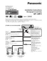
MULTI-COMPACT DISC PLAYER

CDX-P670

X1N/EW

Service
Manual

-

This service manual should be used together with the following manual(s):

Model No.

Order No.

Mech. Module

Remarks

CX-892

CRT2356

C7

CD Mech. Module:Circuit Description, Mech. Description, Disassembly

CONTENTS

1. SAFETY INFORMATION ............................................3

2. EXPLODED VIEWS AND PARTS LIST .......................4

3. BLOCK DIAGRAM AND SCHEMATIC DIAGRAM ...12

4. PCB CONNECTION DIAGRAM ................................22

5. ELECTRICAL PARTS LIST ........................................28

6. ADJUSTMENT..........................................................31

7. GENERAL INFORMATION .......................................38

7.1 DIAGNOSIS ........................................................38

7.1.1 TEST MODE ..............................................38

7.1.2 DISASSEMBLY .........................................44

7.1.3 CONNECTOR FUNCTION DESCRIPTION46

7.2 IC .........................................................................47

7.3 OPERATIONAL FLOW CHART ...........................49

8. OPERATIONS AND SPECIFICATIONS.....................50

Summary of Contents for CDX-P670

Page 1: ...CDX P670 X1N EW Service Manual This service manual should be used together with the following manual s Model No Order No Mech Module Remarks CX 892 CRT2356 C7 CD Mech Module Circuit Description Mech Description Disassembly CONTENTS 1 SAFETY INFORMATION 3 2 EXPLODED VIEWS AND PARTS LIST 4 3 BLOCK DIAGRAM AND SCHEMATIC DIAGRAM 12 4 PCB CONNECTION DIAGRAM 22 5 ELECTRICAL PARTS LIST 28 6 ADJUSTMENT 31...

Page 2: ...l After removing the transport screw cover the hole with the supplied seal CD Player Service Precautions 1 For pickup unit CXX1285 handling please refer to Disassembly see page 44 During replacement handling precautions shall be taken to prevent an electrostatic discharge protection by a short pin 2 During disassembly be sure to turn the power off since an internal IC might be destroyed when a con...

Page 3: ...of 13cm from the focus lens must be kept 2 During repair or tests do not view laser beam for 10 seconds or longer 2 A CLASS 1 LASER PRODUCT label is affixed to the rear of the player 3 The triangular label is attached to the mechanism unit frame CLASS 1 LASER PRODUCT 4 Specifications of Laser Diode Specifications of laser radiation fields to which human access is possible during service Wavelength...

Page 4: ...4 CDX P670 2 EXPLODED VIEWS AND PARTS LIST 2 1 PACKING 9 8 11 12 11 15 12 19 17 10 7 13 5 4 3 1 6 2 14 18 16 ...

Page 5: ...MC 8 Polyethylene Bag CEG1042 7 Polyethylene Bag CEG1099 9 Carton CHG4278 10 Contain Box CHL4278 11 Protector CHP2133 12 Protector CHP2134 13 Seal CNM5599 14 1 Owner s Manual CRD3318 14 2 Owner s Manual CRD3319 14 3 Warranty Card CRY1157 15 Magazine Assy CXB6518 16 Angle Assy CXB3591 17 Cord CDE5830 18 Caution Card CRP1090 19 Caution Card CRP1232 PACKING SECTION PARTS LIST Mark No Description Part...

Page 6: ...6 CDX P670 2 2 EXTERIOR ...

Page 7: ...r Unit CWX2512 14 Screw BMZ26P060FMC 15 Terminal CN902 CKF1059 16 Plug CN901 CKS 460 17 Connector CN921 CKS3407 18 Connector CN911 CKS3831 19 Holder CNC8055 20 Holder CNC8056 21 Grille Assy CXB6823 22 Door CAT2198 23 Door CAT2199 24 Lower Case Unit CXB7005 25 CD Mechanism Module C7R2 CXK4850 26 Screw IMS20P030FZK 27 Screw IMS26P040FMC 28 Transistor Q910 2SD2396 29 Caution Card CRP1232 EXTERIOR SEC...

Page 8: ...8 CDX P670 2 3 CD MECHANISM MODULE ...

Page 9: ...late CNC8375 44 Cover CNC8434 45 Sheet CNM6009 46 Spacer CNM6428 47 Sheet CNM6296 48 PCB CNP5227 49 PCB CNP5228 50 Ball CNR1189 51 Gear CNR1531 52 Belt CNT1086 53 Gear CNV5472 54 Gear CNV5473 55 Rail CNV5920 56 Lever CNV6091 57 Gear CNV5477 58 Arm CNV5478 59 Holder CNV5480 60 Guide CNV5921 61 Guide CNV5922 62 Holder CNV5483 63 Holder CNV5484 64 Clamper CNV5485 65 Gear CNV5486 66 Gear CNV5562 67 Ho...

Page 10: ...5FZK 92 Pickup Unit Service CXX1285 93 94 95 Screw IMS26P040FMC 96 Screw JFZ20P025FNI 97 Photo transistor Q851 PT4800 98 Spring Switch S851 S853 CSN1051 99 LED D851 CN504 2 100 Spring Switch S852 CSN1052 Mark No Description Part No ...

Page 11: ...11 CDX P670 2 4 MAGAZINE ASSY 1 Magazine Assy CXB6518 2 Label CRW1415 3 Tray CNV5341 MAGAZINE ASSY SECTION PARTS LIST Mark No Description Part No ...

Page 12: ... xtal XTAL L_OUT LD VREF adena cs 23 16 24 IPIN IPOUT IPPW POWER XIN XOUT 13 15 98 asens bsens reset CDMUTE ELVREF CONT ELVPVO ejsw mag disk TRP DSP 11 94 93 74 75 3 X202 16 93MHz X701 10 00MHz IC 301 BA5986FM IC 302 LB1836M VDD IC 701 PD5638A A CD CORE UNIT Q851 D851 D SWITCH PCB E MOTOR PCB C S853 S801 S803 V EVREF GND EPVO L 4 3 7 5 11 8 9 2 1 10 17 12 27 16 15 5 15 4 3 4CH SERVO DRIVER MOTOR D...

Page 13: ... Q770 VDD IC 705 TC7SH32F IC 702 LC35256FT 70U SRAM IC 703 HA12187FP IP BUS DRIVER IC 704 PAJ002A CN701 16 B POWER UNIT 10 7 1 Q942 Q911 BUP Q941 BUP BUP BUP Q910 LOUT 3 CDMUTE 6 BP BUSP LCH 5 BUSM 8 ASENB 5 BM 7 ASNB 4 SVC 1 VD POWER VD VD VD POWER 9 B 13 BSENIN CN911 IP BUS OUT CN921 L901 BUP GND BATT GND 3 2 1 CN901 FUSE 2A 10 8 2 17 16 Q912 S802 VR801 EPVO LINEAR POSITION SENSOR ER 1 2 3 CN902...

Page 14: ...AMP SE MOTO 4CH SER CN801 CN802 M853 CXB4421 M851 CXB3003 M854 CXB3004 CSN1052 CSN1051 CSN1051 CN504 2 PT4800 PICKUP UNIT SERVICE CXX1285 C MECHANISM PCB SWITCH PCB D MOTOR PCB E 3 2 CD MECHANISM MODULE Note When ordering service parts be sure to refer to EXPLODED VIEWS AND PARTS LIST or ELECTRICAL PARTS LIST A1 2 C D E ...

Page 15: ...ed as 2 2 2R2 0 022 R022 The mark found on some component parts indicates the importance of the safety factor of the part Therefore when replacing be sure to use parts of identical designation Symbol indicates a resistor No differentiation is made between chip resistors and discrete resistors NOTE Symbol indicates a capacitor No differentiation is made between chip capacitors and discrete capacito...

Page 16: ...16 CDX P670 1 2 3 4 1 2 3 4 D C B A SYSTEM CONTROLLER A 1 2 A2 2 ...

Page 17: ...17 CDX P670 5 6 7 8 5 6 7 8 D C B A SRAM IP BUS DRIVER B CN911 A2 2 ...

Page 18: ...v 9 CH2 TD 0 5V div Test mode 32 tracks jump REV 0 5ms div 8 CH1 TE 0 5V div 9 CH2 TD 0 5V div Test mode Single jump REV 0 5ms div 8 CH1 TE 0 5V div 9 CH2 TD 0 5V div Test mode 100 tracks jump REV 5ms div 6 CH1 FE 0 1V div 3 CH2 FD 0 2V div Normal mode Play 20ms div 3 CH1 FD 0 5V div 0 CH2 MD 1V div Normal mode Focus close 12cm 0 5s div 3 CH1 FD 0 5V div 0 CH2 MD 1V div Normal mode Focus close 8cm...

Page 19: ... 5µs div Normal mode Play 8 CH1 TE 1V div CH2 TEC 1V div Test mode Focus close Tracking open 2ms div 8 CH1 TE 0 5V div 6 CH2 FE 0 5V div Normal mode AGC after focus close 0 2s div 20ms div SCKO 2V div 1µs div Normal mode Play DOUT 2V div 10µs div Normal mode Play LRCK 2V div 20µs div Normal mode Play VD 5V div 50ms div Normal mode No disc GND REFO REFO GND REFO REFO REFO REFO REFO REFO REFO REFO R...

Page 20: ...V div Normal mode During AGC 1 CH1 RFI 1V div CH2 HOLD 5V div Normal mode The defect part passes 800µm B D 500µs div 1ms div 0 5ms div 3 CH1 FD 1V div CH2 HOLD 5V div Normal mode The defect part passes 800µm B D 0 5ms div 9 CH1 TD 0 1V div CH2 HOLD 5V div Normal mode The defect part passes 800µm B D 0 5ms div REFO REFO REFO REFO REFO REFO REFO REFO REFO REFO REFO REFO ...

Page 21: ...8V REG MUTE CN701 B POWER UNIT A 2 2 3 3 POWER UNIT CEK1033 21 CDX P670 1 2 3 4 1 2 3 4 D C B A B ...

Page 22: ...NIT A 4 PCB CONNECTION DIAGRAM 4 1 CD CORE UNIT NOTE FOR PCB DIAGRAMS 1 The parts mounted on this PCB include all necessary parts for several destination For further information for respective destinations be sure to check with the schematic dia gram E E IC Q ADJ M M852 ELV B CN911 C CN801 E F REFO EREF EPVO 1 25 26 50 51 75 76 100 A ...

Page 23: ...23 CDX P670 1 2 3 4 1 2 3 4 D C B A E E E IC Q RESET EJECT MAG SIDE B CD CORE UNIT A A ...

Page 24: ...24 CDX P670 1 2 3 4 1 2 3 4 D C B A B SIDE A 4 2 POWER UNIT A CN701 IP BUS POWER UNIT B CORD ...

Page 25: ...25 CDX P670 1 2 3 4 1 2 3 4 D C B A B SIDE B POWER UNIT B ...

Page 26: ...26 CDX P670 1 2 3 4 1 2 3 4 D C B A 4 4 SWITCH PCB SWITCH PCB D C 4 3 MECHANISM PCB A CN101 E D MECHANISM PCB C M M854 CRG M M851 SPDL HOME TRP DSP D851 PICKUP UNIT SERVICE C D ...

Page 27: ...27 CDX P670 1 2 3 4 1 2 3 4 D C B A 4 5 MOTOR PCB MOTOR PCB E E C ...

Page 28: ... 16S752J R 307 RS1 16S103J R 308 RS1 16S752J R 309 RAB4C332J R 311 RS1 16S102J R 701 RS1 16S681J R 702 RS1 16S102J R 703 RS1 16S222J R 704 RS1 16S104J R 705 RS1 16S104J R 706 RS1 16S222J R 707 RS1 16S104J R 708 RS1 16S0R0J R 715 RS1 16S473J R 716 RS1 16S103J R 717 RS1 16S473J R 718 RS1 16S681J R 719 RS1 16S0R0J R 721 RS1 16S222J R 722 RS1 16S222J R 724 RS1 16S681J R 725 RS1 16S222J R 726 RS1 16S10...

Page 29: ...22 CKSRYB103K25 C 724 CKSRYB471K50 C 801 CKSRYB103K25 C 802 CKSRYB104K16 C 803 CKSRYB103K25 Unit Number CWX2512 Unit Name Power Unit MISCELLANEOUS Q 910 Transistor 2SD2396 Q 911 Transistor IMD2A Q 912 Transistor IMX1 Q 941 Transistor FMG12 Q 942 Transistor IMD2A D 901 Diode 1SR139 400 D 902 Diode 1SR139 400 D 910 Diode HZS6L B1 D 941 Diode MA152WA L 901 Choke Coil 1mH CTH1047 RESISTORS R 901 RS1 1...

Page 30: ...53 Motor Unit TRAY CXB4421 Miscellaneous Parts List Pickup Unit P8 Service CXX1285 M 851 Motor Unit SPINDLE CXB3003 M 852 Motor Unit ELV CXB3006 M 854 Motor Unit CARRIAGE CXB3004 VR 801 Volume 10kΩ B CCW1023 Circuit Symbol and No Part Name Part No E ...

Page 31: ...s filters and wiring required for measurements Before proceeding to further adjustments and mea surements after switching regulator ON let the player run for about one minute to allow the circuits to stabi lize Since the protective systems in the unit s software are rendered inoperative in test mode be very careful to avoid mechanical and or electrical shocks to the sys tem when making adjustment ...

Page 32: ...nd TRK buttons move the pickup unit to the innermost track 3 Press key 9 to close focus the display should read 91 Press key 9 2 times Enter Rough Servo mode Press key 8 to implement the tracking balance adjustment the display should now read 81 4 As shown in the diagram above monitor the LPF outputs using the oscilloscope and check that the phase differ ence is within 75 Refer to the photographs ...

Page 33: ...33 CDX P670 Grating waveform 45 0 75 60 30 90 Echt Xch 20mV div AC Fcht Ych 20mV div AC ...

Page 34: ...loscope One L P F Measuring Points EREF EPVO Setting Without a magazine in Test mode With the mechanism placed upside down Place the CD mechanism module so that the CD core unit is above Confirmation Procedure 1 Enter Test mode then select Multi CD player 2 Press key 7 to enter Mechanism Test mode 3 Press key 12 twice to specify the amount of movement 6 3 ADJUSTMENT OF ELEVATION WHEN THE CD CORE U...

Page 35: ...CD core unit below Take care not to short cir cuit the PCB 11 Confirm the height of the stage Use the DISC key to select Disc No 3 Check if the stopper bend of the clamp lever is engaged in the groove of the frame stopper Fig 2 4 Note The stopper bend will be pressed downward into the groove for final clamping Confirm the engagement position of the stopper bend If the stopper bend is engaged in th...

Page 36: ...rease the volt age of EREF adjusted in step 8 by 20 mV 13 Place the mechanism horizontal Go back to step 11 to reconfirm the stage height 14 When adjustment of the stage height is completed proceed as fol lows 15 Press the EJECT switch 16 Once operation of the mechanism has stopped turn the power OFF 17 Wait more than one minute after the power is turned off then turn the power ON and insert a mag...

Page 37: ...the clamp lever Frame stopper OK Engaged in the center and pressed downward NG Fig 1 Dislocated toward the first CD Adjust the insertion gate of magazine to the third scale E 1 2 3 4 6 Dislocated toward the sixth CD Fig 2 Fig 3 Fig 4 ...

Page 38: ...leasing the key CRG move and 100TR jump operations are brought into the Tracking close sta tus when the key is released Powering Off On resets the jump mode to Single TR 91 the RF AMP gain setting to 0 dB and the auto matic adjustment value to the initial value During exchanging discs do not press the keys for the discs to be exchanged The following head units are exceptional so that their enterin...

Page 39: ...isplay T Close and F T AGC and RF AGC and Fit Servo Display Power ON Not adjustment for T Offset Display Display 8 RF AMP Gain Select 8 Power OFF Power OFF Power OFF 8x 8x 8x TRK SEC MIN 9x 9x 9x TRK SEC MIN 8x 8x 8x TRK SEC MIN 9x 9x 9x TRK SEC MIN or 8x 8x 8x TRK SEC MIN 9x 9x 9x TRK SEC MIN or 00 00 00 TRK SEC MIN 99 99 99 TRK SEC MIN or 00 00 00 TRK SEC MIN 99 99 99 TRK SEC MIN or 00 00 00 TRK...

Page 40: ...inner diameter CRG can t be moved from inner diameter Failure on home switch or CRG move mechanism 11 Electricity Focus Servo NG Focusing not available Stains on rear side of disc or excessive vibrations on REWRITABLE 12 Electricity Spindle Lock NG Spindle not locked Sub code is strange not readable Failure on spindle stains or damages on disc or excessive vibrations Subcode NG A disc not containi...

Page 41: ...uble analysis 1 Shifting to the New Test Mode 1 Turn on the current test mode by starting the reset from the 4 and 6 keys together 2 Select M CD for the source through the specified procedure including use of the SOURCE key Then press the 12 key while maintaining the regulator turned off 3 After the above operations the new test mode remains on irrespective of whether the M CD is turned on or off ...

Page 42: ...tup Status No Contents Protective action 00 CD 5V ON process in progress None 01 Servo LSI initialization 1 3 in progress None 02 Servo LSI CRAM initialization in progress None 03 Servo LSI initialization 2 3 in progress None 04 Offset adjustment 1 3 in progress None 05 Offset adjustment 2 3 in progress None 06 Offset adjustment 3 3 in progress None 07 FZD adjustment in progress None 08 Servo LSI ...

Page 43: ...s closed Off focus Carriage closing in progress 41 Focus tracking AGC started Off focus 42 Focus AGC started Off focus 43 Focus AGC in progress Off focus 44 Tracking AGC in progress Off focus 45 Standing by after focus tracking AGC are over Off focus 46 Spindle processes applicable servo Off focus 47 Check for servo close is started Off focus 48 Check of LOCK pin started Off focus or spindle not l...

Page 44: ...emove the Upper Case Removing the CD Mechanism Module Fig 5 Remove the four dampers Remove the two springs Disconnect the connector and then remove the CD Mechanism Module Fig 6 CD Mechanism Module Fig 5 Power Unit Removing the Door 1 Remove the Door A in the direction of arrow2 while pushing the Grille in the direction of arrow1 the slide is done as it is in the direction of arrow3 and remove the...

Page 45: ...or assy were soldered 5 Remove the two screws and lift the mechanism PCB up as shown in the figure on the upper right At this time make sure that the motor PCB and flexible relay card are not pulled excessively 6 Remove screw A and then remove the carriage motor assy lighting conductor feed screw holder feed screw and belt see Fig 10 7 Remove screw B on the main side and the pickup unit together w...

Page 46: ...46 CDX P670 7 1 3 CONNECTOR FUNCTION DESCRIPTION 8 9 10 11 5 6 7 1 2 3 4 1 BUS 2 GND 3 GND 4 NC 5 BUS 6 GND 7 LCH 8 ASENB 9 RCH 10 SGNDR 11 SGNDL 1 2 3 1 GND 2 ACC 3 BATT IP BUS POWER SUPPLY ...

Page 47: ...AMSW I L 26 FMPCB I Pull down 27 SIMUKE I Pull down 28 NC Not used 29 IPIN I Data input from IP BUS interface IC 30 IPOUT O C Data output for IP BUS interface IC 31 32 NC Not used 33 FMIPSW I H 34 testin I Test program mode input 35 XSO O C CD LSI data output 36 XSI I CD LSI data input 37 XSCK O C CD LSI clock output 38 M6M12 I 6 12 disc select input 39 43 NC Not used 44 rd O C SRAM enable output ...

Page 48: ...C detect timing input 92 disk Disc detector input 93 ELVPVO Voltage input from ELV position sense 94 ELVREF ELV reference voltage input 95 TRP I Tray position input 96 AVSS A D GND 97 VDIN Power supply short sensor input 98 VREF I A D converter reference voltage input 99 AVCC A D VCC 100 EPCS I O C E2PROM detect input Chip select output PD5638A Format Meaning C C MOS 30 31 50 51 80 81 100 1 LC3525...

Page 49: ... Pin10 adena L Pin3 VD IN Pin96 1 3V VD IN 2 1V mag L DISC Search POWER L Pin10 asens Pin19 POWER H Pin10 adena L Pin3 VD IN Pin96 1 3V VD IN 2 1V POWER L Stand by Error message A0 Error message A0 Start the CD player Source Multi CD YES asens L 7 3 OPERATIONAL FLOW CHART ...

Page 50: ...her product refer to the supplied Installation manuals of both products and connect cords that have the same function General System Compact disc audio system Usable discs Compact Disc Signal format Sampling frequency 44 1 kHz Number of quantization bits 16 linear Power source 14 4 V DC 10 8 15 1 V allowable Max current consumption 1 0 A Weight 1 9 kg 4 2 lbs Dimensions 248 W 66 H 168 D mm 9 3 4 W...

Reviews: