Zener Diodes
Publication date: April
2006
SKE
00022
CED
1
MALS068X
Silicon planar type
For constant voltage and surge absorption circuits
Features
Bi-directional and high electrostatic discharge ESD
Small terminal capacitance C
t
Absolute Maximum Ratings
T
a
=
25
aa
°
C
Parameter
Symbol
Rating
Unit
Repetitive peak forward current
I
FRM
200
mA
Total power dissipation
*
1
P
T
150
mW
Junction temperature
T
j
TT
150
°
C
Storage temperature
T
stg
TT
–
55
to +
150
°
C
Electrostatic discharge
*
2
ESD
±
15
kV
Note) *
1
: P
T
=
150
mW achieved with a printed circuit board.
*
2
: Test method: IEC
61000
-
4
-
2
(C =
150
pF, R =
330
Ω
, Contact discharge:
10
times)
Electrical Characteristics
T
a
=
25
aa
°
C
±
3
°
C
Parameter
Symbol
Conditions
Min
Typ
Max
Unit
Zener voltage
*
V
Z
V
V
I
Z
=
5
mA
ZZ
6
.
5
7
.
0
7
.
5
V
Zener operating resistance
R
Z
R
R
I
Z
=
5
mA
ZZ
20
Ω
Reverse current
I
R
V
R
=
4
.
0
V
R
R
50
nA
Terminal capacitance
C
t
V
R
=
0
V, f =
1
MHz
R
R
15
pF
Note)
1
. Measuring methods are based on JAPANESE INDUSTRIAL STANDARD JIS C
7031
measuring methods for diodes.
2
. The temperature must be controlled
25
°
C for V
Z
mesurement.
V
Z
value measured at other temperature must be adjusted to V
Z
(
25
°
C)
3
. *: V
Z
guaranted
20
ms after current fl ow.
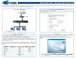
Unit : mm
1 : Cathode
2 : Cathode
EIAJ : SC-79
SSMini2-F1 Package
0.80
+0.05
–0.03
0.60
+0.05
–0.03
0.12
+0.05
–0.02
1.20
+0.05 –0.03
0
+0
–0.05
0.30
±
0.05
0.01
±
0.01
1.60
±
0.05
0.01
±
0.01
1
2
0.80
±
0.05
(0.80
)
(0.60
)
(0.15
)
(0.60
)
5
°
5
°
RX
Internal Connection
1
2
This product complies with the RoHS Directive (EU 2002/95/EC).