background image

© Panasonic System Networks Co., Ltd. 2011 
Unauthorized copying and distribution is a violation 
of law.

ORDER NO. KM41106439CE

Telephone Equipment

Model No.

KX-TG4111MEB
KX-TG4112MEB
KX-TGA410MEB

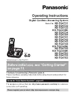
Digital Cordless Phone

B: Black Version 
(for Mexico)

Caller ID Compatible

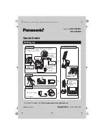
Configuration for each model

   Model No 

Base Unit 

Handset  Charger Unit  Expandable

KX-TG4111  1 (TG4111)  1 (TGA410)                           Up to 6

KX-TG4112  1 (TG4111)  2 (TGA410) 

Up to 6

Information for optional accessories

You can expand your phone system by registering optional 
handsets (KX-TGA660ME) to a single base unit.
Optional handsets and the supplied handset are different model 
so that some functions may not be available.
Refer to each Operating Instruction for details.

(Handset)

KX-TGA410MEB

KX-TG4111MEB

(Base Unit)

(Charger Unit)

Summary of Contents for KX-TG4111MEB

Page 1: ...ch model Model No Base Unit Handset Charger Unit Expandable KX TG4111 1 TG4111 1 TGA410 Up to 6 KX TG4112 1 TG4111 2 TGA410 1 Up to 6 Information for optional accessories You can expand your phone system by registering optional handsets KX TGA660ME to a single base unit Optional handsets and the supplied handset are different model so that some functions may not be available Refer to each Operatin...

Page 2: ... Diagrams Circuit Board Diagrams Exploded Views and Replacement Parts List It is essential that these critical parts should be replaced with manufacturer s specified parts to prevent shock fire or other hazards Do not modify the original design without permission of manufacturer IMPORTANT INFORMATION ABOUT LEAD FREE PbF SOLDERING If lead free solder was used in the manufacture of this product the ...

Page 3: ...sassembly Instructions 41 11 2 How to Replace the Handset LCD 45 12 Measurements and Adjustments 46 12 1 Equipment Required 46 12 2 The Setting Method of JIG 46 12 3 Adjustment Standard Base Unit 50 12 4 Adjustment Standard Charger Unit 51 12 5 Adjustment Standard Handset 52 12 6 Things to Do after Replacing IC or X tal 53 12 7 Frequency Table 55 13 Miscellaneous 56 13 1 How to Replace the LLP Lea...

Page 4: ... the instructions 2 2 About Lead Free Solder PbF Pb free Note In the information below Pb the symbol for lead in the periodic table of elements will refer to standard solder or solder that contains lead We will use PbF solder when discussing the lead free solder used in our manufacturing process which is made from Tin Sn Silver Ag and Copper Cu This model and others like it manufactured using lead...

Page 5: ...Bi Please check the manufacturer s specific instructions for the melting points of their products and any precautions for using their product with other materials The following lead free PbF solder wire sizes are recommended for service of this product 0 3 mm 0 6 mm and 1 0 mm 2 3 Discarding of P C Board When discarding P C Board delete all personal information such as telephone directory and call...

Page 6: ... Approx 77 mm x 126 mm x 90 mm Approx 140 g Rechargeable Ni MH battery AAA R03 size 1 2 V 550 mAh Super Heterodyne PLL synthesizer Quadrature Discriminator 13 824 MHz 100 Hz Frequency Modulation 40 bit Tone DTMF Pulse Up to 48 digits Up to 24 digits Phonebook 11 days at Standby 13 hours at Talk 0 C 40 C 20 80 relative air humidity dry Approx 159 mm x 49 mm x 29 mm Approx 130 g Base Unit Handset Ch...

Page 7: ...erformed Handset doesn t make up duplex in no free RF channels because of interference 1 Dummy Bearer Base unit sends Dummy data to the all stand by state handsets Handsets receive that data for synchronization and monitoring request from the base unit Base unit doesn t send Dummy bearer in no free RF channels because of interference 1 Note 1 It is a feature under FCC 15 regulation and for interfe...

Page 8: ...digital data RXDATA BBIC IC1 converts RXDATA into a voice signal and outputs it to speaker Transmission Handset A voice signal from microphone is encoded to digital data and converted into a 1 9GHz modulated radio signal by BBIC IC1 The RF signal after which is amplified in BBIC is fed to an antenna Base unit As for a base unit RF RF signal is received in two antennas BBIC IC501 compares RF signal...

Page 9: ...LL DETECT HOOK BELL Q111 LIN LOUT RF_PART HSMIP HSMIN IC501 BBIC INUSE DETECT 2 INUSE DETECT 1 RECEIVE AMP DCIN 1 DCIN 2 IC302 VCCPA VBAT_APU VBAT VCC_FE VCC_IF VCC_VCO PDN DET 3 0V DOUBOUT SCL SDA WP IC611 EEPROM MEMORY R151 R152 R131 R133 Q171 VBAT KEY 1 KEY C 3 0 V REGULATOR STM CKM R371 R372 VCCA VCC KX TG4111 4112 BLOCK DIAGRAM Base Unit_Main ANT2 ANT1 RXp RXn RXON TXp TXn TXON RESET RSTN ...

Page 10: ...10 KX TG4111MEB KX TG4112MEB KX TGA410MEB 4 3 Block Diagram Base Unit_RF Part KX TG4111 4112 BLOCK DIAGRAM Base Unit_RF Part DA801 ANT2 ANT1 TXON RXON RXp RXn ANT2 ANT1 TXp TXn ...

Page 11: ...Caller ID demodulation The BBIC implements monitor and demodulate the FSK DTMF signals that provide CID information from the Central Office Digital Switching The voice signal from telephone line is transmitted to the handset or the voice signal from the handset is transmitted to the Telephone line etc They are determined by the signal path route operation of voice signal Block Interface Circuit RF...

Page 12: ...or peripherals and analog part is insulated from VBAT by Doubler of BBIC Circuit Operation 5 5V VBAT RSTN Reset pin 54 VBAT pin 10 pin 57 pin 9 pin 15 IC501 IC302 IC611 BBIC DOUBLER OUT For peripherals VDDC 1 2V AC Adaptor 3 0V REGULATOR EEPROM Receive Amp 3 0V STM CKM RF Part Startmonitor IC501 57pin VDDC 1 2 V VBAT Reset RSTN IC501_54 pin BBIC chip initialize CKM STM ...

Page 13: ...13 KX TG4111MEB KX TG4112MEB KX TGA410MEB 4 4 3 1 Charge Circuit The voltage from the AC adaptor is supplied to the charge circuits D362 R372 R371 D361 CHARGE F301 DCP CHARGE C306 5 5V DCM ...

Page 14: ... current flow T L101 D101 Q141 Q161 R163 R167 D101 L102 P101 R ON HOOK Circuit Q141 is open Q141 is connected as to cut the DC loop current and to cut the voice signal The unit is consequently in an on hook condition Pulse Dial Circuit Pin 6 of BBIC turns Q141 ON OFF to make the pulse dialing Side Tone Circuit Basically this circuit prevents the TX signal from feeding back to RX signal As for this...

Page 15: ...age is monitored at pin 17 of IC501 There is no parallel connection if the voltage is 0 54 V or higher while a parallel connection is deemed to exist if the voltage is lower Parallel connection detection when off hook When off hook the voltage is monitored at pin 18 of IC501 the presence absence of a parallel connection is determined by detecting the voltage changes If the Auto disconnect function...

Page 16: ...dulated in an FSK Frequency Shift Keying format Data 1 is a 1200 Hz sine wave and data 0 is a 2200 Hz sine wave There are two types of the message format which can be received i e the single message format and plural message format The plural message format allows to transmit the name and data code information in addition to the time and telephone number data Also the telephone exchange service pr...

Page 17: ...MARK data pass the following route Telephone Line P101 L101 L102 C121 C122 R121 R122 IC501 25 24 If the unit deems that a telephone connected in parallel is in use ACK is not returned even if CAS is received and the information for the second and subsequent callers is not displayed on the portable handset display CAS CAS CPE Alerting Signal Dual Tone of 2130 Hz 2750 Hz 15 dBm 900 ohm load 80 5 ms ...

Page 18: ...TP SPOUTN CKM STM CKM STM BBIC RESET CHG_CTL CHG_DET WP CLK DATA KEYSTOROBE_A E KEYIN_1 5 CHARGE Q4 D7 MIC Receiver LED Monitor SP LCD KEYS RF part ANT1 X1 13 824 MHz EEPROM VBAT BATTERY Q5 RSTN BELL VBAT VBAT 3V 4 0V VBAT 4 0V IC4 RXn RXp RXON TXp TXn TXON KX TGA410 BLOCK DIAGRAM Handset KEY_LED Q6 LED KEY LCD ...

Page 19: ...19 KX TG4111MEB KX TG4112MEB KX TGA410MEB 4 6 Block Diagram Handset_RF Part KX TGA410 BLOCK DIAGRAM Handset_RF Part DA801 TXON RXON RXp RXn ANT TXp TXn ...

Page 20: ...3 Setting data is stored e g ID user setting 4 7 2 Power Supply Circuit Reset Circuit Circuit Operation When power on the Handset the voltage is as follows BATTERY 2 2 V 2 6 V BATT F1 BBC1 IC1 10 pin The Reset signal generates IC1 54 pin and 1 8 V Startmonitor IC1 57pin VDDC 1 2 V VBAT Reset RSTN IC1_54 pin BBIC chip initialize CKM STM GND BATTERY 2CELL BBIC 3 0V 3 0V DOUBLER OUT Charge Pump For a...

Page 21: ...o Fig 101 in Power Supply Circuit Reset Circuit P 12 4 7 4 Battery Low Power Down Detector Circuit Operation Battery Low and Power Down are detected by BBIC which check the voltage from battery The detected voltage is as follows Battery Low Battery voltage V Batt 2 35 V 50 mV The BBIC detects this level and starts flashing Power Down Battery voltage V Batt 2 1 V 50 mV The BBIC detects this level a...

Page 22: ... Charge control is executed at handset side so that the operation when using charger is also controlled by handset Refer to Circuit Operation Handset P 20 The route for this is as follows DC pin of J1 F1 R1 CHARGE pad Handset CHARGE pad DC pin of J1 R1 TP1 TP2 J1 AC Adaptor F1 ...

Page 23: ...01 L102 P101 T R TEL LINE T R TEL LINE L101 P101 L102 C121 C122 R121 R122 IC501 24 25 T R TEL LINE L101 P101 L102 R111 R112 C111 C112 Q111 IC501 5 HANDSET MIC R73 74 C11 13 RA4 IC1 22 23 HANDSET_RF_TX_ROUTE ANT ANT BASE_UNIT_RF_RX_ROUTE IC501 46 47 28 R181 C184 Q161 Q141 D101 L101 L102 P101 T R TEL LINE T R TEL LINE L101 P101 L102 D101 Q141 R165 C173 Q171 C178 R178 IC501 16 44 45 BASE_UNIT_RF_TX_R...

Page 24: ...ating Instructions Instruction book on TSN Server 6 Installation Instructions Refer to the Operating Instructions Note You can download and refer to the Operating Instructions Instruction book on TSN Server 7 Operating Instructions Refer to the Operating Instructions Note You can download and refer to the Operating Instructions Instruction book on TSN Server ...

Page 25: ... 7262 7664 PANA SONI see letters printed on dial keys See next page 5 Enter ٨ ٨ ٨ ٨ Address 1 6 Enter 㧖 㧖 New Data 1 4 Select Write EEP using or then press or V Default Data INT Caller List V V Initial setting BACK V Set tel line BACK BACK V Set dial mode Select Set tel line using or then press or V Service Mode Read EEP Write EEP Set Addr M CLEAR SELECT INT SELECT SELECT SELECT SELECT SELECT SELE...

Page 26: ... cause serious damage to the computer system ID 00 02 00 06 Given value Desired Number hex Input Keys Desired Number hex Input Keys 0 0 A Flash 0 1 1 B Flash 1 C Flash 2 D Flash 3 E Flash 4 9 9 F Flash 5 7 Press a long confirmation beep will be heard 8 Press to return to standby mode After that turn the base unit power off and then power on New Data BACK CLEAR _ _ _ _ _ _ Set Addr Set Addr M M OFF...

Page 27: ...irmation beep will be heard 8 Press to return to standby mode After that remove and reinsert the batteries Press the Power button for about 1 second if the power is not turned on 6 Enter 㧖 㧖 New Data 1 4 Select Write EEP using or then press or V OFF Default Data New Data M Caller List V V Initial setting V Service Mode Read EEP Write EEP Set Addr _ _ _ _ _ _ Set Addr Set Addr Ringer setting M INT ...

Page 28: ...rm the contents Careless rewriting may cause serious damage to the handset Items Address Default Data New Data Possible Adjusted Value MAX hex Possible Adjusted Value MIN hex Remarks Battery Low 00 12 00 13 00 00 2 Frequency 00 07 00 08 00 01 ID 00 02 00 06 Given value Desired Number hex Input Keys Desired Number hex Input Keys 0 0 A Flash 0 1 1 B Flash 1 C Flash 2 D Flash 3 E Flash 4 9 9 F Flash ...

Page 29: ...0MEB 9 Service Mode 9 1 How to Clear User Setting Handset Only Handset Press simultaneously until a beep sound is heard Then single handset is initialized The contents of user setting are reset to factory default Usage time is not cleared ...

Page 30: ...t Transmission P 40 Check Handset Reception P 40 Check Caller ID P 40 Power ON Base Unit OK FLOW CHART Check Power Range Check the RF part Handset Voice Transmission Check Handset Transmission Handset Voice Reception OK OK OK Check Handset Reception Caller ID function Check Caller ID Caller ID Error No voice No voice No charge Not working NG No link OK Link Battery Charge OK Check Battery Charge C...

Page 31: ...to AC outlet 1 Is output voltage of AC adaptor 5 5 V YES Check AC Adaptor Check VDDC 1 2 V Test Point VDDC OK Check Power Supply Circuit NO NO NO NO RSTN Reset High YES Check Reset Circuit Check Xtal CLK 13 824 MHz YES Check X501 Check BBIC Check Power Supply Circuit Reset Circuit Check X1 C8 C9 Is the voltage of TP 3 0 V about 3 0 V Is the voltage of TP VBAT 2 3 V more Check the battery and aroun...

Page 32: ...er source Charge Handset on Base Unit Is the voltage of two charge contacts about 3 V or more OK NO Check Charge Contacts at Base Unit from mechanical point of view YES Is BBIC IC1 34 high at charge state Check Charge Circuit Check Power of Handset Is Check Power OK NO NO YES Check Charge Circuit of Charger Unit Check Handset Plug in the AC Power source Charge Handset on Charger Unit Is the voltag...

Page 33: ... then check the TP_CKM IC501 57pin To adjust frequency send command SFR until the frequency counter becomes13 824 MHZ 55HZ Check around Power Supply Circuit Adjust 3 0V voltage to 3 0 V Does Base Unit make link with normal working Handset Check around X501 and RF module and adjust clock frequency NO NO NO NO YES YES Is the voltage of VBAT about 3 0 V Check the RF part Does the RF clock CLK oscilla...

Page 34: ...To adjust frequency send command SFR until the frequency counter becomes13 824 MHz 55HZ Check around Power Supply Circuit Reset Circuit Adjust 3 0V Vottage to 3 0V Does Handset make link with Base Unit Correct working unit Check around X1 and RF module and adjust clock frequency NO NO NO NO Is the voltage of TP VBAT about 2 2 2 8 V Is the voltage of TP VDDC about 1 8 V YES YES YES YES Is the volta...

Page 35: ...2 2 a Re register regular HS Normal mode to base unit to be checked If this operation fails in some ways the base unit is defective b Re register handset to be checked to regular BU Normal mode If this operation fails in some ways the handset is defective Base unit is defective Handset is defective START Registration of Regular HS to base unit Registration of handset to Regular BU other checkings ...

Page 36: ... Please refer to the each item Note 1 Refer to Check Link P 33 Start Link confirmation Normal 1 Control signal confirmation X tal Frequency confirmation TX confirmation Range confirmation Normal TEST RANGE Check Check BBIC interface parts RF Block BBIC on BU HS P C B Adjust X tal Frequency 1 Check TX Block GOOD 5 2 3 4 OK OK OK NG NG NG NG NG OK OK ...

Page 37: ...ustment Check X tal Frequency 10 368 MHz 100Hz Check X tal Frequency 13 824 MHz 100 Hz 3 TX confirmation HS Mode HS_Burst Mode 1 BS Mode BS_Burst Mode 2 1 Remove wire antenna 2 and connect spectrum analyzer to TP 3 2 Confirm TX power whether spec is satisfied Power 14 5dBm 1 Connect spectrum analyzer to TP 4 2 Confirm TX power whether satisfied spec Power 16 0dBm 4 Range Confirmation Normal HS BU ...

Page 38: ...3 At distance of about 20m between HS and BU Link OK TX Power of the HS is OK No Link TX Power of the HS is NG Range Confirmation RX TEST RX sensitivity check HS BU setting Checked unit High TX power 1 Regular unit Low TX power 1 1 Register Regular HS to BU to be checked 2 Set TX Power of the BU and the Regular HS according to CHART1 3 At distance of about 20m between HS and BU Link OK RX Sensitiv...

Page 39: ...eat this step The next step must be completed within 90 seconds 3 Handset Press OK then wait until a long beep sounds Note While registering En La Base Modo Registro is displayed on all registered handsets When you purchase an additional handset refer to the additional handset s installation manual for registration MENU i 1 3 0 L A handset can cancel its own registration to the base unit or other ...

Page 40: ...tion Caller ID Call Waiting Caller ID P 16 Note Make sure the format of the Caller ID service of the Telephone company that the customer subscribes to It is also recommended to confirm that the customer is really a subscriber of the service Check MIC of handset Check handset Tx in Signal Route Check speaker of handset Check handset Rx in Signal Route YES Did bell ring Message indicator blinks Chec...

Page 41: ...nd Assembly Instructions 11 1 Disassembly Instructions 11 1 1 Base Unit Ԙ Remove the 4 screws to remove the cabinet cover ԙ Remove the tape and solders Ԛ Remove the screw to remove the jack holder Cabinet cover Jack holder Ԙ 4 screws Tape and Solders ԙ Ԛ screw ...

Page 42: ...42 KX TG4111MEB KX TG4112MEB KX TGA410MEB ԛ Remove the screw to remove the main P C board Main P C board ԛ screw ...

Page 43: ...the cabinet body and the cabinet cover then pull it along the gap to open the cabinet Ԛ Likewise open the other side of the cabinet ԛ Remove the cabinet cover by pushing it upward Ԝ Remove the solders ԝ ԝ Remove the screw to remove the main P C board Main P C board Ԝ Screw Cabinet cover Cabinet body Cabinet cover 2 screws Ԙ Solders ...

Page 44: ...TG4111MEB KX TG4112MEB KX TGA410MEB 11 1 3 Charger Unit Ԙ Remove the screw to remove the cabinet cover ԙ Remove the solders to remove the 2 charge terminals Ԙ Screw ԙ Solders Main P C board 2 charge terminals ...

Page 45: ... not damaged Fit the heatseal of a new LCD Rubber of Soldering Iron Part No PQZZ430PRB Tip of Soldering Iron Part No PQZZ430PIR Heatweld with the tip of the soldering iron about 5 to 8 seconds in case of 60W soldering iron New LCD 0 2 mm 0 2 mm P C board If interval tolerance between center lines is less than 0 2 mm it is o k Horizontal Interval Tolerance Vertical Interval Tolerance OK NG NG NG Ho...

Page 46: ...t like a mass production 12 2 The Setting Method of JIG Preparation Serial JIG cable PQZZ1CD300E PC which runs in DOS mode Batch file CD ROM for setting PNZZTG4131ME Note If you have the JIG Cable for TCD500 series PQZZ1CD505E change the following values of resistance Then you can use it as a JIG Cable for both TCD300 and TCD500 series It is an upper compatible JIG Cable 12 2 1 Connections Base Un...

Page 47: ...T and BATT Connect the JIG cable GND black to GND Connect the JIG cable UTX yellow to UTX and URX red to URX Note COM port names may vary depending on what your PC calls it DC Power or Battery 2 GND black 3 To Serial Port com port 1 JIG Cable PC URX red 3 UTX yellow Handset P C board 1 BATT BATT GND UTX URX ...

Page 48: ...ssages appear change the port number or 䇭check the cable connection 䊶If any value appear go to next step 7 Type DOSKEY then press the Enter key Example C Documents and Settings D D CD PNZZTG D PNZZTG SET_COM X D PNZZTG READID 00 52 4F A8 A8 D PNZZTG DOSKEY D PNZZTG Example error happens C Documents and Settings D D CD PNZZTG D PNZZTG SET_COM X D PNZZTG READID ޓ CreateFile error ERROR 10 Can t open...

Page 49: ...ess wreeprom Write the data of EEPROM Type wreeprom 01 23 45 01 23 is address and 45 is data to be written bs_burst Base unit outputs RF power in burst test mode on antenna 2 Type bs_burst tx_high Keep TX power high Type tx_high tx_low Keep TX power low Type tx_low Command name Function Example rdeeprom Read the data of EEPROM Type rdeeprom 00 00 FF and the data from address 00 00 to FF is read ou...

Page 50: ... D113 D153 D133 D473 D472 Q171 C115 C121 C126 C112 C114 C122 C163 C176 C175 C173 C132 C351 C601 C670 C301 C523 C120 C123 C124 C664 C666 C662 C472 C473 C475 C510 C530 C513 C512 C514 C331 URX UTX 5 5V UGND R111 R115 R122 R176 R175 R172 R133 R131 L1T L1R CL1 ANT2 CL2 R506 TMS TCK TDI TDO RSTN STM CKM P15 R505 R604 R503 R511 VCCA VREF VBAT VBG 3 0V VDDC RTCK R332 R331 DCM DCP SPP SPN L663 L476 L474 L6...

Page 51: ...X TGA410MEB 12 4 Adjustment Standard Charger Unit When connecting the simulator equipment for checking please refer to below 12 4 1 Bottom View A PNLB1922Z 3 0A F1 PbF IG Charge Charge 12 2 W Digital Volt Meter DC POWER DC 5 5 V GND ...

Page 52: ... C H G _ D E T C H G _ C T R L S P P H O N E VREF GND_J TDO TCK TMS TDI VBG C13 C97 C1 C19 C75 C74 C113 X1 BATT BATT CHG CHG R69 R68 R807 R7 R64 R562 R34 R28 R27 R10 R45 R2 R3 R73 R74 L9 IC4 IC3 RA4 RA3 RA2 D22 D21 ANT_TP D3 D4 Q4 Q2 Q3 C8 C81 C71 C70 C9 C99 C7 C825 C45 C46 C43 C863 C895 C897 C826 C25 C22 C504 C127 C73 C86 C33 C57 C10 C78 C79 C121 C80 C15 C5 C147 C3 F1 C4 C150 R35 R1 R561 R501 R50...

Page 53: ...ing Method of JIG P 46 Items How to download Required adjustment EEPROM IC611 Adjusted parameter data is stored in memory country version batch file default batch file etc 1 Change the address 0001 of EEPROM to 55 to download the data 2 Default batch file Execute the command default bat 3 Country version batch file Execute the command TG4111US_WW_RevXXX_YYY bat 1 4 Clock adjustment X tal X1 System...

Page 54: ...ersion batch file default batch file etc 1 Default batch file Execute the command default bat 2 Default batch file remaining Execute the command TGA410US_DEF_RevXXX_YYY bat 2 3 Country version batch file Execute the command TGA410US_WW_RevXXX_YYY bat 2 4 Clock adjustment 5 2 35 V setting and battery low detection X tal X1 System clock 1 Apply 2 6V between BATT and BATT with DC power 2 Input Comman...

Page 55: ...55 KX TG4111MEB KX TG4112MEB KX TGA410MEB 12 7 Frequency Table Ch hex TX RX Frequency MHz Channel 0 00 1928 448 Channel 1 01 1926 720 Channel 2 02 1924 992 Channel 3 03 1923 264 Channel 4 04 1921 536 ...

Page 56: ...efficiently choose the right sized nozzle of the hot air desoldering tool that matches the IC package Be careful about the temperature of the hot air desoldering tool not to damage the PCB and or IC 13 1 3 How to Remove the IC 1 Heat the IC with a hot air desoldering tool through the P C Board 2 Pick up the IC with tweezers etc when the solder is melted completely Note Be careful not to touch the ...

Page 57: ...When placing the IC the positioning should be done very carefully 3 Heat the IC with a hot air desoldering tool through the P C Board until the solder on IC bottom is melted Note Be sure to place it precisely controlling the air volume of the hot air desoldering tool 4 After soldering confirm there are no short and open circuits with visual inspection Solder Soldering Iron P C Board Land IC Solder...

Page 58: ...amage the PCB foil Flux Recommended Flux Specific Gravity 0 82 Type RMA lower residue non cleaning type Note See About Lead Free Solder PbF Pb free P 4 13 2 2 How to Remove the IC 1 Put plenty of solder on the IC pins so that the pins can be completely covered Note If the IC pins are not soldered enough you may give pressure to the P C board when cutting the pins with a cutter 2 Make a few cuts in...

Page 59: ...acy of the IC setting with the corresponding soldering foil 2 Apply flux to all pins of the FLAT PACKAGE IC 3 Solder the pins sliding the soldering iron in the direction of the arrow 13 2 4 How to Remove a Solder Bridge 1 Lightly resolder the bridged portion 2 Remove the remaining solder along the pins using a soldering iron as shown in the figure below ...

Page 60: ...D5S B1ACGP000008 3 2 1 4 C0DBEYY00102 Reverse View Cathode Anode B0DDCD000001 ψ ψ 1SS355 PQVDPTZT2530 Anode Cathode B0ECKM000008 1 88 67 23 44 22 66 45 1 4 8 5 PNWIGA410MER Anode Cathode MA8043 C B E B1ADCF000040 B1GBCFYY0010 B1ABDF000017 Reverse View Anode Cathode B3ACB0000216 C2HBCY000081 Anode Cathode B0DDCD000001 1 88 67 23 44 22 66 45 Reverse View B1ABGE000011 1 3 2 4 5 6 C0DBZYY00357 Reverse...

Page 61: ...grams may be modified at any time with the development of new technology 14 1 3 Charger Unit Schematic Diagram Charger Unit Notes 1 DC voltage measurements are taken with voltmeter from the negative voltage line 2 The schematic diagrams may be modified at any time with the development of new technology Important Safety Notice Components identified by mark have special characteristics important for...

Page 62: ...516 0 1u C805 2 7p GND TXON R806 470 RXp LCD_CS LCD_VDD LCD_RST LCD_CD LCD_SCL LCD_SIO LCD_GND WBX02 AP1 10pin PARALLEL WIRE R502 33 TCK URX TDI RTCK TMS UTX TDO UGND C670 NC WBX01 AP1 10pin PARALLEL WIRE C652 NC SW1 LOCATOR 1 2 NC KEYIN2 KEYS_C C660 NC KEYS_D C653 NC KEYS_E C654 NC ANS_LED MSG_LED LED_VDD VBAT C655 NC KEYIN3 KEYIN1 C656 NC C651 NC L661 NC L662 NC L663 NC L664 NC R651 NC R652 NC L...

Page 63: ...1 C142 K0 01u L474 NC C165NC C115 0 22u C164 NC RA504 68 1 2 3 4 C504 1u C185 NC R151 100k C181 NC L1T C507 K2 2u 3 0V R172 100k Q141 B E C 3 0V CHARGE C514 0 1u 5 5V C331 NC R331 68k C351 1u VBG C110 NC C114 NC R115 27k R511 NC R510 10k C341 330u 6 3 C306 100u SA103 NC 2 1 3 IN 2 OUT1 1 ADJ 4 OUT2 D142 30V AK Q111 B C E Q171 B C E D133 A K D153NC A K D113 A K D361 NC AK C161 10u C511 10u C503 10u...

Page 64: ...T 4 0V IC4 1 VOUT 2 GND 4 CN 5 VCC 3 SHD 6 CP C58 1 0uF VBAT R562 NC 3 0V 4 0V R563 0 C2 220u 6 3 C10 220u 6 3 C1 220u 6 3 Q9 C150 0 1u C23 0 1u C24 1u C188 1u C32 1u C84 NC GND L6 C34 39p Q2 C19 1000p Q3 R9 30k R8 3 3 R2 30k Q4 R6 10k CN3_C 5 A0 CN3_C 2 OTP_PWR CN3_C 9 VDDA CN3_C 3 CS1 CN3_C 12 GND CN3_C 11 V0 CN3_C 7 SI CN3_C 6 SCL CN3_C 4 RES CN3_C 10 VSS CN3_C 8 VDD CN3_C 1 GND C56 1 0uF C57 1...

Page 65: ...98 NC C99 NC GND GND C896 1 8p C805 2 4p C806 2 4p C810 2 5p C813 1 6p C812 8 2n L809 1p C811 100p C822 10p C826 10p C825 10p C897 24p C37 10u R35 100k 3 0V X1 13 824M C73 10p C72 10p GND GND L13 180n L14 NC C86 22u L9 0 R28 2 2k GND ANT_TP MIC AP1 1 2 ANT Short GND ANT Short R10 10 D21 4 3V D14 4 3V D13 4 3V D22 4 3V MIC POWER RECEIVER RECEIVER W 0 2mm L 3 8mm 1st layer Test Pattarn for Carbon Sp...

Page 66: ...66 KX TG4111MEB KX TG4112MEB KX TGA410MEB 14 4 Schematic Diagram Charger Unit J1 2 1 G TP1 TP2 F1 R1 6 8 2W SCHEMATIC DIAGRAM Charger Unit ...

Page 67: ...2 DA801 Q651 Q141 C652 C660 C654 C651 C656 C653 C655 C165 C164 SA101 SA103 C894 P101 C508 C509 C505 C506 C172 C503 C501 C524 C810 C322 C321 C893 C805 C813 C812 C859 C896 C519 C518 C516 C515 C826 X501 R652 R651 R807 R161 R164 R145 R144 R151 R892 R160 R512 R501 R509 R322 R321 R657 R655 R656 SW1 R507 R806 R891 R372 L809 NC2 KEYS_E KEYS_C LCD_BLT1 LCD_GND LCD_RST LCD_CS LCD_CD LCD_SIO LCD_SCL LCD_VDD ...

Page 68: ...51 C601 C670 C301 C523 C120 C123 C124 C664 C666 C662 C472 C473 C475 C510 C530 C513 C512 C514 C331 URX UTX 5 5V UGND R111 R115 R122 R176 R175 R172 R133 R131 L1T L1R CL1 ANT2 CL2 R506 TMS TCK TDI TDO RSTN STM CKM P15 R505 R604 R503 R511 VCCA VREF VBAT VBG 3 0V VDDC RTCK R332 R331 DCM DCP SPP SPN L663 L476 L474 L661 L665 IC601 IC611 RA151 D361 Q111 Q161 Q652 KX TG4111 4112 CIRCUIT BOARD Base Unit_Mai...

Page 69: ... VREF GND_J TDO TCK TMS TDI VBG C13 C97 C1 C19 C75 C74 C113 X1 BATT BATT CHG CHG R69 R68 R807 R7 R64 R562 R34 R28 R27 R10 R45 R2 R3 R73 R74 L9 IC4 IC3 RA4 RA3 RA2 D22 D21 ANT_TP D3 D4 Q4 Q2 Q3 C8 C81 C71 C70 C9 C99 C7 C825 C45 C46 C43 C863 C895 C897 C826 C25 C22 C504 C127 C73 C86 C33 C57 C10 C78 C79 C121 C80 C15 C5 C147 C3 F1 C4 C150 R35 R1 R561 R501 R504 orange green R23 R806 R67 R66 R24 R31 R33 ...

Page 70: ...112MEB KX TGA410MEB 15 2 2 Bottom View SP DOWN LEFT RIGHT UP TALK OFF SOFT2 SOFT1 CN3_C LED2 LED5 LED3 MENU LED4 LED12 LED1 LED8 LED7 LED9 LED6 FLASH A MIC 0 8 7 4 1 5 6 2 3 9 KX TGA410 CIRCUIT BOARD Handset_Main Bottom View ...

Page 71: ...B KX TG4112MEB KX TGA410MEB 15 3 Circuit Board Charger Unit 15 3 1 Component View 15 3 2 Bottom View R1 J1 CIRCUIT BOARD Charger Unit Component View A A PNLB1922Z 3 0A F1 PbF IG CIRCUIT BOARD Charger Unit Bottom View ...

Page 72: ...72 KX TG4111MEB KX TG4112MEB KX TGA410MEB 16 Exploded View and Replacement Parts List 16 1 Cabinet and Electrical Parts Base Unit 10 A A Ref No Figure A 2 6 x 8 mm PCB1 7 2 5 A A 1 5 4 8 3 6 9 ...

Page 73: ...HHR 4MRT is available through sales route of Panasonic 3 Attach the SPACER No 115 to the exact location described above 102 103 104 E105 E104 E101 1 110 111 105 108 E108 B 116 115 3 101 107 E102 E107 E109 B E106 MIC100 PCB100 106 112 109 Ref No Ǿ2 8 mm B Figure 114 113 2 Spacer No 115 Battery cover Put it in the center Stick it between ribs CUSHION RUBBER STICK IT WITHIN THE FRAMEWORK ON P C B E10...

Page 74: ...74 KX TG4111MEB KX TG4112MEB KX TGA410MEB 16 3 Cabinet and Electrical Parts Charger Unit B 200 200 1 200 3 200 4 200 2 PCB200 ...

Page 75: ...75 KX TG4111MEB KX TG4112MEB KX TGA410MEB 16 4 Accessories P1 P2 1 Note 1 The illustrations differ from the actual gift box and cushion A2 A1 ...

Page 76: ...r Type ECFD Semi Conductor ECQS Styrol ECUV PQCUV ECUE Chip ECQMS Mica ECCD ECKD ECBT F1K ECUV Ceramic ECQE ECQV ECQG Polyester ECEA ECST EEE Electlytic ECQP Polypropylene Wattage Type Voltage Of Capacitor 10 16 1 8W 14 25 1 4W 12 1 2W 1 1W 2 2W 3 3W Voltage ECQ Type ECQG ECQV Type 05 50V 1 100V 2 200V ECSZ Type 0J 6 3V 1A 10V 1C 16V 1E 25 25V 1V 35V 50 1H 50V 1J 16V 2A 100V 0F 3 15V 1A 10V 1V 35V...

Page 77: ...05 ECJ1VB0G106M 10 S C506 ECUV1A105KBV 1 C507 ECUV1A225KBV 2 2 C508 ECUE1H100DCQ 10p C509 ECUE1H120JCQ 12p C510 ECUV1A105KBV 1 C511 ECJ1VB0G106M 10 S C512 ECUE1A104KBQ 0 1 C513 ECUV1A225KBV 2 2 C514 ECUE1A104KBQ 0 1 C515 ECUV1A105KBV 1 C516 ECUE1A104KBQ 0 1 C517 ECUE1A104KBQ 0 1 C518 ECUE1A104KBQ 0 1 C519 ECUE1A104KBQ 0 1 C520 ECUE1A104KBQ 0 1 C521 ECUE0J105KBQ 1 C522 ECUE1H100DCQ 10p C530 ECUE1H1...

Page 78: ...A104KBQ 0 1 C8 ECUE1H100DCQ 10p C9 ECUE1H120JCQ 12p Safety Ref No Part No Part Name Description Remarks C10 EEE0JA221WP 220 C11 ECUE1A104KBQ 0 1 C12 PQCUV0J106KB 10 C13 ECUE1A104KBQ 0 1 C15 ECUE1H390JCQ 39p C17 ECUE1H100DCQ 10p C18 ECUE1H100DCQ 10p C19 ECUE1H102KBQ 0 001 C20 ECJ1VB0G106M 10 S C21 ECUV1A105KBV 1 C22 ECUE1A104KBQ 0 1 C23 ECUE1A104KBQ 0 1 C24 ECUE0J105KBQ 1 C25 ECUV1A225KBV 2 2 C26 E...

Page 79: ...PLATE RTL for KX TG4112MEB 200 1 PNKM1204Z1 CABINET BODY PS HB 200 2 PNJT1066Z CHARGE TERMINAL 200 3 PNKF1150Z1 CABINET COVER PS HB 200 4 PQHA10023Z RUBBER PARTS FOOT CUSHION Safety Ref No Part No Part Name Description Remarks PCB200 PNWPTGA660CH MAIN P C BOARD ASS Y RTL JACK J1 K2ECYB000001 JACK S RESISTOR R1 ERX2SJ6R8 6 8 FUSE F1 K5H302Y00003 FUSE Safety Ref No Part No Part Name Description Rema...

Reviews: