SERVICE MANUAL
PORTABLE MINIDISC RECORDER
No.20911
Jan. 2001
COPYRIGHT 2001 VICTOR COMPANY OF JAPAN, LTD.
XM-R700SL
XM-R700SL
Area Suffix
US
Singapore
Contents
Safety Precautions
Important for laser products
Attention when
MD pick up is exchanged
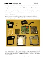
Disassembly method
Adjustment method
Maintenance of laser pickup
Replacement of laser pickup
Description of major ICs
1-2
1-3
1-4
1-5
1-15
1-17
1-17
1-18~37
Summary of Contents for XM-R700SL
Page 40: ...2 2 XM R700SL M E M O ...
Page 46: ...XM R700SL 3 2 M E M O ...