background image

SERVICE MANUAL

SPECIFICATIONS AND PARTS ARE SUBJECT TO CHANGE FOR IMPROVEMENT

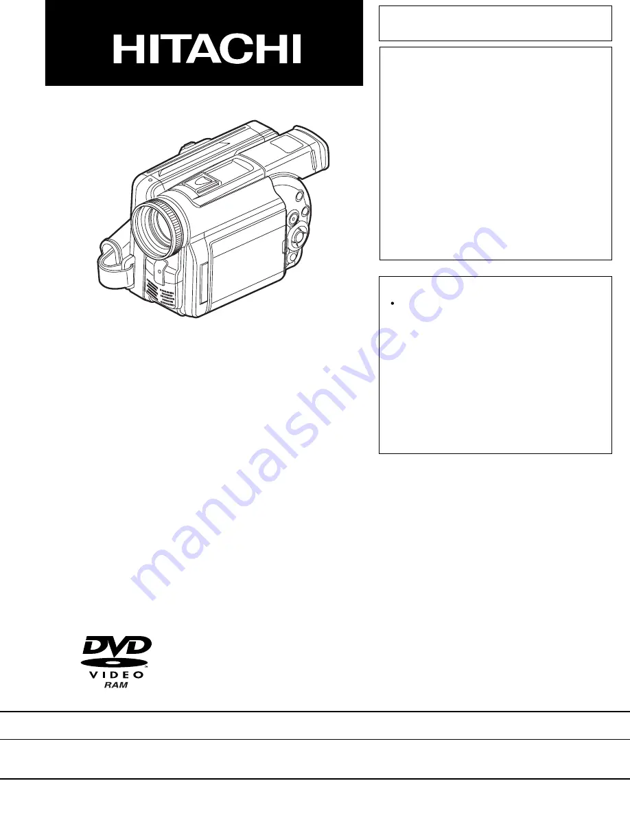
DVD VIDEO CAMERA/RECORDER

April 2002

SM7202

DZMV238EAU
DZMV238ESW
DZMV230E
DZMV230EUK
DZMV208EAU
DZMV208ESW
DZMV200E
DZMV200EUK

Contents included

This service manual does not include
information on drive mechanism unit and
MAN circuit board.
When servicing, replace the entire drive
mechanism unit or the entire MAN circuit
board if necessary.
For fault judgement, see Chapter 6 simplified
circuit board diagrams that show the voltage
values of major ICs on circuit boards (DRC
and HDM) mounted on drive mechanism unit
and MAN circuit board.

Digital Media Division

Summary of Contents for DZMV200E

Page 1: ...cluded This service manual does not include information on drive mechanism unit and MAN circuit board When servicing replace the entire drive mechanism unit or the entire MAN circuit board if necessary For fault judgement see Chapter 6 simplified circuit board diagrams that show the voltage values of major ICs on circuit boards DRC and HDM mounted on drive mechanism unit and MAN circuit board Digi...

Page 2: ...cs and the parts list in this Service Manual The use of a substitute replacement component which does not have the same safety characteristics as the HITACHI recommended replacement one shown in the parts list in this Service Manual may create shock fire or other hazards Product safety is continuously under review and new instructions are issued from time to time For the latest information always ...

Page 3: ...rength causing malfunctions Cautions when using lead solder When replacing components remove the lead free solder previously used for soldered points as far as possible For additional soldering melt lead free solder completely and mix well with lead solder Do not perform repair using the bare soldering iron tip without adding solder Soldering iron for servicing It is recommended that you use a sol...

Page 4: ...cation 5 All tolerances other than 5 are indicated in schematic diagrams No indication 1 8W 1 16W for leadless resistors without indication All capacitances other than the above are indicated in schematic diagrams Capacitors Item Value Dielectric strength Indication No indication µF P pF No indication 50V All dielectric strengths other than 50V are indicated in schematic diagrams Item Value Indica...

Page 5: ... Block 2 4 1 8 EVF Block 2 4 2 Before Starting Disassembly 2 5 3 Troubleshooting during Disassembly 2 6 3 1 Removing DVD RAM DVD R disc 2 6 CONTENTS 1 4 Disassembly Procedure 2 8 4 1 Top cover R block L block and Front block 2 9 4 2 Disc cover 2 10 4 3 LCD case U MR circuit board LCD block AUD circuit board Adjustment cap and L case 2 11 4 4 Rear block REF circuit board Camera block MAN circuit bo...

Page 6: ...0 1 Error messages during picture control system adjustment 3 26 10 2 Error messages during autofocus system adjustment 3 27 10 3 Error messages during stabilizer adjustment 3 28 10 4 Error messages during spot noise adjustment 3 28 CHAPTER 4 EXPLODED VIEW 1 Cabinet 1 4 1 2 Cabinet 2 4 2 3 Camera 4 3 4 LCD Monitor 4 3 5 Electronic Viewfinder EVF 4 4 6 Accessories 4 4 CHAPTER 5 REPLACEMENT PARTS LI...

Page 7: ...c approx 36 to 120 minutes XTRA 1 approx 60 minutes FINE approx 120 minutes STD approx 30 minutes FINE approx 60 minutes STD 1998 Video Movie Conforming to DVD video recording format MPEG audio layer 2 Photo Still Simultaneous recording conforming to DVD video recording format 704 480 pixels and JPEG Video Movie Conforming to DVD video format MPEG audio layer 2 MPEG audio layer 2 Dolby AC3 Linear ...

Page 8: ...76 XTRA FINE mode 352 576 STD mode Camera External input 704 480 XTRA FINE mode 352 480 STD mode Camera 704 480 XTRA FINE mode 352 480 STD mode 2 Video audio analog signal input function Provided Not provided Provided Not provided 3 8 cm DVD RAM disc one side type of accessory Provided Not provided Reference Specifications of DZ ACE1 AC Adapter 100 240 V AC 50 60 Hz 28 VA at 100 V 8 4 V 1 5 A Appr...

Page 9: ...meter Minimum required illumination Minimum recordable distance Viewfinder LCD monitor Image stabilizer system Shutter When recording speed video movie When recording photo still Flash Self timer recording Interval recording Built in microphone Recording playback media Recording 8 cm DVD RAM disc mode 8 cm DVD R disc Maximum 8 cm DVD RAM disc video both sides movie recordable time 8 cm DVD R disc ...

Page 10: ... mm Refer to 2 on page 1 2 Output 1 1 ø 3 5 mm stereo mini jack impedance 600 to 1 k ohm 1 mini USB Type B Lithium ion 7 2 V DC approx 5 8 W when recording with LCD monitor off approx 82 x 101 x 143 mm excluding hood and projections 0 to 40 C 80 or less 0 to 30 C when connected to PC approx 670 g Equipped video audio input output jack used or Not equipped Refer to 2 on page 1 2 Equipped 1 6 modes ...

Page 11: ...table shows the differences in Disc Navigation function between DZ MV238E MV230E MV208E MV200E and DZ MV100E using the function names of DZ MV238E MV230E MV208E MV200E Since the names of functions using Disc Navigations are different for DZ MV238E MV230E MV208E MV200E and DZ MV100E some functions overlap and are omitted in the following table Note A DVD RAM disc recorded or edited on DZ MV238E MV2...

Page 12: ... 1 0 2 6GB DVD RAM 12cm 4 7GB DVD RAM 12cm Version 2 1 4 7GB 1 46GB DVD RAM 12cm 8cm DVD RAM DVD Digital Versatile Disc Version 1 0 DVD R 3 95GB DVD R 12cm 4 7GB 1 46GB DVD R 12cm 8cm DVD ROM DVD Video DVD Audio DVD RW 4 7GB DVD R 12cm DVD R for General Version 2 0 DVD R for Authoring Version 2 0 4 Note the following three types of 12 cm DVD RAM disc depending on whether the cartridge is provided ...

Page 13: ...en considered difficult It also defines the devices for achiev ing the characteristics inherent in disc such as easy arrangement of playback order play list function coping with photos stills recording of character data for searching etc 2 DVD video format The conventional DVD video format was adopted only for playback only DVD ROM discs i e DVD video discs but it was revised in 2002 and also appl...

Page 14: ...et of that at right None MPEG 2 program stream Possible Not needed Players and PCs compatible with DVD RAM Coding format Number of streams Aspect ratio Number of pixels NTSC Photo still data structure Coding format Number of streams Number of channels per stream Coding format Number of streams Display control command DVD video format 720 480 704 480 352 480 352 240 Not defined Up to 8 Mono Stereo ...

Page 15: ...en designate it when Disc Navigation is in operation Tilt up down to left or right to move to an item and press the center of joystick to designate the item Operational procedure 1 Release write protect of DVD RAM disc to be initialized and load the disc in the DVD video camera recorder 2 Press the DISC NAVIGATION button to start Disc Navigation 3 Press the MENU button to display the menu screen 4...

Page 16: ...a menu item and designate it when Disc Navigation is in operation Tilt up down to left or right to move to an item and press the center of joystick to designate the item Operational procedure 1 Load the DVD R disc to be finalized in the camera recorder 2 Press the DISC NAVIGATION button to start Disc Navigation 3 Press the MENU button to display the menu screen 4 Choose Disc Finalize on the menu s...

Page 17: ...ote With DVD RAM disc the remaining capacity on only one side will appear The remaining capacity of write protected DVD RAM disc will appear as 0 min Before starting Use the joystick to move the cursor to a menu item and then designate it when the Disc Navigation is in operation Tilt up down to left or right to move to an item and press the center of joystick to designate the item Operational proc...

Page 18: ...e caddy and then follow the instructions of device to be used Insert bare disc disc removed from caddy or cartridge into caddy or cartridge before using it on DVD video camera recorder 6 1 Disc packed in cartridge 1 Removing the disc 1 Release snap off the lock pins at the bottom left corners of sides A and B see Fig 6 1a Use a fine tipped pen to slide the lock pin in the direction of arrow and th...

Page 19: ...the disc at its edge and center hole and remove it in the direction of arrow obliquely upward 2 Replacing the disc in caddy 1 Hold the disc at its edge and center hole with the printed label surface up Fig 6 2b 2 Insert the disc under the claws at the disc hold portion in the direction of arrow Gently push the disc in until it is completely stored Fig 6 2a Fig 6 2b 2 1 3 CLAWS 1 2 3 ...

Page 20: ...s depending on the country or district Prohibition Do not short circuit battery terminals Do not disassemble or modify the battery Do not throw the battery into fire 7 1 Checking charged status The charged status can be checked using the CHARGE ACCESS indicator Charging 0 to 50 complete Blinks once per 1to 2 seconds Charging 50 to 70 complete Blinks twice per 1 to 2 seconds Charging 75 or more Bli...

Page 21: ... without a disc loaded is left without being operated for at least 3 minutes after it is turned on except during playback recording 2 During the demo mode the recording indicator blinks and no operation other than the following is accepted Power switch Stop cancel button DISC EJECT button MEMO button DISC NAVIGATION button 3 The demo mode will not operate when the camera recorder is connected to P...

Page 22: ... item Disc animation Displaying logo Displaying concept Disc animation Displaying logo Playback using Disc Navigation Creating play list using Disc Navigation Disc animation Displaying logo Displaying features Description Displays animation in which the disc at the center rotates at gradually higher speed The DVDCAM logo appears first while it extends to left and right and then the Hitachi logo ap...

Page 23: ... operations 1 Items to be reset The items of system reset in the above item except for the date function will be reset 2 How to reset Before starting Use the joystick to move the cursor to a menu item and then designate it when the Disc Navigation is in operation Tilt up down to left or right to move to an item and press the center of joystick to designate the item Operational procedure 1 Press th...

Page 24: ... be normally performed because of dirt of fingerprints dust etc or warped disc is loaded Appears when finalizing of disc cannot be normally performed because of dirt of fingerprints dust etc or warped disc is loaded Appears if accident such as power off has occurred during finalizing If the message still appears even when the disc is cleaned and finalized again the disc may be defective Appears if...

Page 25: ...mber of recorded scenes has reached the upper limit 999 of format 4 Appears if an attempt is made to divide move or delete a scene after the number of recorded scenes has reached the upper limit 999 of format 4 5 This message also appears when the number of scenes exceeds 999 by division or movement Turn power on again or reload a disc following the screen Check the DVD video camera recorder and r...

Page 26: ...can be repaired only when AC adapter is connected This message also appears if AC adapter is not connected when finalizing DVD R disc Appears if mismatch has occurred between the recorded video and the scene information because editing was performed near the limit of disc storage capacity on any device made by other manufacturers it also appears if the control information file was operated Appears...

Page 27: ...the upper limit 999 defined by the format Appears if an attempt was made to change the Video recording mode of recorded DVD R disc using the camera menu Once even one scene is recorded on DVD R disc which has been initialized it will be specified that the originally designated Video record mode be maintained Choose YES following screen and designate A thumbnail will be automatically produced if it...

Page 28: ...VD RAM or DVD R disc a message will appear on the monitor LCD If such a message is displayed refer to Explanation of Trouble Message in this chart and perform appropriate troubleshooting 4 Letters in brackets in check point columns show the circuit board where the check point is located and the side of the board Example 1 MAN A shows that the check point is located on side A of MAN circuit board E...

Page 29: ...Referring to Disassembly remove the top cover and then separate the R and L blocks 2 Remove the AUD circuit board and microphone referring to Disassembly 3 Connect the AUD circuit board to R block MAN circuit board 4 Connect the microphone to AUD circuit board 5 Remove the two screws holding the SWL circuit board one screw holding the speaker and then remove the SWL circuit board and speaker from ...

Page 30: ... IC1502 faulty Replace MAN circuit board NG IC0501 or its peripheral circuits faulty NG F0001 fuse faulty Replace F0001 NG Replace JK0001 or DCJ circuit board NG Connector connections faulty OK Replace L case speaker NG IC6101 or its peripheral circuits faulty NG IC6101 or its peripheral circuits faulty OK Check parts on AVJ circuit board NG Connector connections faulty OK Replace microphone NG Ch...

Page 31: ...crophone connection faulty JK6003 contact faulty NG Check Q6001L R and their peripheral circuits on AVJ circuit board NG Replace MAN circuit board or check C6112L R and C6154L R OK IC6101 or its peripheral circuits faulty NG Check switch SW3105 or SW3106 OK Replace MAN board NG Replace L case SWL circuit board OK PG6101 73 operation changes voltage NG Replace disc cover zoom switch OK IC1506 or it...

Page 32: ...sc is inserted Disc cartridge is write protected Normally initialized disc was inserted Check CCD sensor drive pulses Check CCD output signal Image appears in LCD or EVF 0V when AV output cable is connected Replace MAN circuit board Yes Replace MAN circuit board No Check connections between MAN circuit board and drive mechanism unit Check connections between MAN circuit board and drive mechanism u...

Page 33: ...rresponding circuit board diagrams schematic circuit diagrams Note The diagrams in this section show only the locations of test lands TL They are not schematic or circuit board diagrams that show the information of mounted components For information on mounted components check the corresponding schematic and circuit board diagrams 1 TL positions on REF circuit board 1 Side A TL0501 TL0506 TL0503 T...

Page 34: ...0 TL0505 To MAN UNIT CN1501 S SW 0 8 0 2 2 0 8 0 TL0004 TL0508 TL0512 TL0504 TL0501 TL0503 TL0510 TL0505 TL0506 To EBLB PG3953 5 1 3 2 0 0 5 0 4 5 TL3719 2 Side B 3 Schematic diagrams for reference Regulator EVF ...

Page 35: ...T TL3604 To MAN UNIT PG1501 TL6109 TL6110 To SWITCH UNIT TL6131 23 22 21 20 19 18 17 16 15 TL3604 2 TL positions on AUD circuit board 1 Side A 3 Schematic diagrams for reference 3 TL position on LCD circuit board 1 Circuit board 2 Schematic diagram for reference ...

Page 36: ...n 1 2 3 4 5 6 7 8 9 10 11 12 13 14 1 3 4 5 6 7 9 10 13 14 2 11 12 8 13 AV output jack PC connection terminal TO PC External microphone jack Viewfinder DISC EJECT button Press down this button to open the disc guide CHARGE ACCESS indicator Will blink or light during charging or while the DVD video camera recorder is operating Zoom lever Push the lever to the T side for tel ephoto or to the W side f...

Page 37: ... Volume control buttons VOL buttons To adjust the volume of sound from speaker etc BATTERY EJECT button To release the battery SELECT MENU DISC NAVIGATION DISPLAY VOL RESET LCD BRIGHT EXPOSURE FOCUS 29 31 32 30 32 29 30 31 33 35 36 38 37 34 37 33 34 35 36 38 15 DISPLAY button DIG ZOOM button DISC NAVIGATION button REVERSE SEARCH button STOP button FORWARD SKIP button REC button ZOOM T button ZOOM ...

Page 38: ...ig 1 1 1 Top cover 2 Heat radiating rubber A 3 R block 4 L block 5 O ring 6 Hand strap 7 Disc cover Fig 1 1 1 2 L Block Fig 1 2 1 SWL cable 2 SWL circuit board 3 L case 4 LCD block 5 MR circuit board 6 LCD case U 7 Adjustment cap 8 AUD circuit board 9 Front block 10 Front case 11 Microphone cover 12 Microphone 13 Lens hood Fig 1 2 ...

Page 39: ...lock 4 MAN circuit board 5 REF circuit board 6 Circuit board frame 7 Camera block Fig 1 3 Fig 1 4 1 4 R Block 2 2 Fig 1 4 1 Drive block 2 Lock unit 3 R case 4 Link bracket 5 Loader 6 Drive mechanism unit 7 Heat radiating rubber B 8 Heat radiating rubber C 9 Unit cover 10 Rack spring 11 Lead rack 12 Seek motor ...

Page 40: ...1 Rear cover 2 EVF block 3 Jack cover R 4 Battery terminal 5 DCJ circuit board 6 JACK holder 7 AVJ circuit board 8 Jack cover S Fig 1 5 Fig 1 6 1 6 LCD Block Fig 1 6 1 LCD case B 2 Monitor LCD 3 Monitor backlight 4 LCD frame 5 LCD circuit board 6 LCD case U ...

Page 41: ...ame R 3 Lens frame F 4 Lens 5 Crystal filter 6 Light shading rubber 7 CCD image sensor 8 Lens heat radiating plate Fig 1 7 Fig 1 8 1 8 EVF Block Fig 1 8 1 EVF case U 2 EVF LCD 3 Eyecup 4 Clear cover 5 EVF case B 6 EVF fulcrum 7 EBLB circuit board 8 LCD holder 9 EVF backlight 10 LCD holder cover ...

Page 42: ...After checking and removing the disc close the disc loading block If the disc loading block does not open refer to 3 Troubleshooting during Disassembly on the next page 2 Flat cable connectors female used in this DVD video camera recorder are four types a d shown in Fig 2 1 Note that the disconnection method with flat cable is different for each connector Some connectors have the same structure as...

Page 43: ...s the O ring L will detach automatically Be careful not to lose it Be careful not to damage the front case microphone cable e or its connector 1 Remove the screw holding the top cover 2 Remove the top cover in the direction of the arrow and then remove the heat radiating rubber A M 3 Remove the seven screws holding the L block 4 While opening the L block in the direction of arrow a from the rear r...

Page 44: ...501 and CN1501 from the MAN circuit board 14 Remove the REF circuit board in the direction of the arrow 15 Disconnect the three flat cables on MAN circuit board 16 Remove the three screws holding the camera block 17 Disconnect the two flat cables and the one connector on MAN circuit board 18 Remove the screw holding the MAN circuit board 19 Remove the MAN circuit board in the direction of the arro...

Page 45: ...Jack cover R Drive block MAN circuit board Circuit board frame DRF circuit board Hot shoe SE circuit board CCD image sensor Lens Rear cover Lock unit R case Loader Drive mechanism unit 4 6 Lead rack Rack spring Seek motor 4 Disassembly Procedure This section explains the general disassembly procedure for this DVD video camera recorder For the order of removing components follow the disassembly flo...

Page 46: ...le opening the L block in the direction of arrow a from the rear release the tab and disconnect R and L blocks PG1501 and PG6101 then move the L block in the direction of arrow b to separate it from the R block Front block D 5 Disconnect the connector G on AUD circuit board 6 Move the bottom of front block in the direction of the arrow to release the tab c on the side 7 Release the tab d on the to...

Page 47: ...amage the flat cable a Take care with the tab b on R case E 1 Disconnect the flat cable on the MAN circuit board F 2 Remove the hand strap B from the R case E 3 Remove the four screws holding the disc cover A 4 Remove the disc cover in the direction of the arrow Caution when reinstalling When reinstalling the disc cover take care with the wiring of flat cable a Fig 4 2b When reinstalling the disc ...

Page 48: ...oard in the direction of the arrow LCD block C 6 Disconnect the flat cable on LCD circuit board 7 Remove the screw holding the LCD block 8 Release the tab on LCD case B that hold the LCD block AUD circuit board D 9 Disconnect the two flat cables and one connector on AUD circuit board 10 Remove the three screws holding the AUD circuit board Adjustment cap E L case F 11 Insert a fine tipped flat bla...

Page 49: ... board 6 Remove the REF circuit board in the direction of the arrow Camera block C 7 Remove the screw holding the circuit board frame and ground cable 8 Disconnect the three flat cables on MAN circuit board 9 Remove the three screws holding the camera block MAN circuit board D Circuit board frame E DRF circuit board F 10 Disconnect the one flat cable connector of DRF circuit board and one connecto...

Page 50: ...ive block B 2 Remove the two screws holding the hinge and then open the hinge 3 Disconnect the connector on drive block circuit board Fig 4 5b 4 Remove the three screws holding the drive block Lock unit C R case D 5 Remove the three screws holding the lock unit Caution when reinstalling When installing the lock unit wire the cables a and b of lock unit as shown in Fig 4 5b A Link bracket E Hinge F...

Page 51: ...e block circuit board 4 Remove two screws and then remove the seek motor from drive mechanism unit 5 Remove screw and then remove the lead rack from the drive mechanism unit 6 Remove the rack spring from the lead rack Caution when reinstalling Attach the rack spring in a new lead rack as shown in the figure Do not make scratch tooth on lead rack Because invisible tiny dust on screw shaft of seek m...

Page 52: ...ack cover S and remove the jack holder in the direction of the arrow 4 Remove the jack cover S in the direction of the arrow 5 Widen the portion a of jack holder in the direction of the arrow 6 Remove the AVJ circuit board in the direction of the arrow 7 Remove the DCJ circuit board in the direction of the arrow Jack cover R F 8 Release the two tabs one by one and then remove the jack cover R Batt...

Page 53: ...crew holding lens frame R 2 Remove the two screws holding the SE circuit board 3 Open the gyro side of SE circuit board in the direction of the arrow 4 Remove the two screws holding the SE circuit board and lens 5 Unsolder the points on CCD image sensor 6 Remove the two screws holding the CCD image sensor Lens C 7 Remove the screw holding lens frame F Note during reinstalling The crystal filter do...

Page 54: ... backlight LCD circuit board A 1 Disconnect the flat cable on LCD circuit board 2 Unsolder the three points on LCD circuit board three cables on monitor backlight 3 Remove the screw holding the LCD circuit board LCD frame B monitor backlight C monitor LCD D LCD case B E 4 Release the two stoppers of LCD frame A LCD circuit board B LCD frame C Monitor backlight D Monitor LCD E LCD case B Fig 4 10 ...

Page 55: ... EVF fulcrum 3 Remove the EVF case U in the direction of the arrow EVF case B D EBLB circuit board E EVF LCD F EVF backlight G 4 Remove the EVF LCD block H from EVF case B and then release the two tabs on LCD holder cover J 5 Release the two tabs and then remove the EBLB circuit board 6 Disconnect the two flat cables on EBLB circuit board 7 Remove the EVF LCD and EVF backlight from LCD holder K in...

Page 56: ...operation of camera block including optical system clock battery input output These programs control the DVD disc drive system mecha nism block Remarks Does not require updating Does not require updating 1 1 Checking firmware versions Purpose To display the versions of the following firmware programs stored in the microprocessors of DVD video camera recorder Fig 1 1 System firmware System Camera m...

Page 57: ...firmware Fig 1 2c 5 When all required updating is completed the screen for verifying completion of updating will appear Fig 1 2e The updated firmware will be displayed in red 6 Turn the DVD video camera recorder off and remove the DVD RAM disc for updating 1 1 1 1 1 Not all firmware programs need updating every time The firmware programs that do not require updating will be skipped With this DVD v...

Page 58: ... be deleted 2 Turn the DVD video camera recorder on and then press the DISC NAVIGATION button 3 While the Disc Navigation menu screen is displayed tilt the joystick to right and hold it and then press the following 2 buttons simultaneously to display the debug menu SELECT REC 4 With the debug menu screen Fig 2 1 displayed choose Delete RX file and designate it To restore normal status press the st...

Page 59: ...ordinary initialization is not possible because the data on DVD RAM disc has been destroyed excluding physical damage to disc and Disc Navigation does not start Operational procedure 1 Turn the DVD video camera recorder on and then insert the disc to be initialized 2 Hold down the following 3 buttons simultaneously for at least 3 seconds in the camera image status SELECT REC VOL plus 3 Follow the ...

Page 60: ...the following 2 buttons simultaneously Releasing the buttons will display the detailed information of playback file SELECT MENU To restore normal status press the DISPLAY button Caution Be sure to press the DISPLAY button after the operation is finished Since the playback file detailed information display function is backed up neglecting to press DISPLAY will always display the detailed informatio...

Page 61: ...ode of the trouble that occurred before when the content differs from that of the latest trouble appears on the lower row Each time new trouble that differs from previous ones occurs the error codes will be rewritten from the upper row in sequence If the following problems occur the message shown in Fig 3 2b or 3 2c will appear on the LCD monitor When the self diagnosis function judges that recove...

Page 62: ...ata to disc failed During processing of buffer overflow error writing data to disc failed Troubleshooting 1 Turn the DVD video camera recorder on again take care not to subject the DVD video camera recorder to impact or vibrations when power is supplied again 2 Turn the DVD video camera recorder off remove the disc and then check whether it is physically damaged damage or dirt If there is no abnor...

Page 63: ...ge appears 3 Press the DISPLAY button and release it and then within 0 5 second hold down the following 2 buttons for at least 3 seconds to display the test mode screen Fig 3 2d Has nothing to do with this function DISPLAY SELECT 4 While the test mode screen is displayed press the following 2 buttons simultaneously DISPLAY Stop cancel 5 Press the center of joystick to display the error code detail...

Page 64: ...sory provided 1 Personal Computer will be abbreviated as PC hereafter 2 The actual jig shape may be different from the illustration since it might have been changed to improve workability 3 The filters may be used in 6 3 Shutter Adjustment 1 2 List of charts for adjustment 1 3 Test equipment etc Color video monitor color TV with AV input jacks Oscilloscope Vectorscope 1 Digital voltmeter DVM Frequ...

Page 65: ...ustment program Although this chapter explains the adjustment procedure in accordance with actual PC screens it is also possible to independently adjust one item unless otherwise specified 3 Note that the adjustment program is subject to change without notice for improvements in functions and operability and that the actual displays instructions on PC screen may be different from those in this man...

Page 66: ...o Auto On Off CAMERA Field Off Off Off On Off Remarks Set to 48 after system reset Set to On after system reset Be sure to set to Off since the On setting hinders adjustment Set to Auto after system reset Be sure to set to Off since the Auto of Start setting will hinder adjustment Item Camera Functions Setup Program AE White Bal EIS Dig Zoom Record Functions Setup Input Source PHOTO Input Self Tim...

Page 67: ...nates the drive into which the adjustment floppy disk has been inserted If using a drive other than A designate that drive 3 The number to be input after space designates the serial port number of PC If the PC has two or more serial ports and the RS 232C cable DSP R jig is connected to a port other than serial port 1 input that serial port number 4 If the model select screen does not appear make s...

Page 68: ...veral hundred products several thousand products adjusted at factory during production It is not a value inherent in individual products 4 Perform the Spot Noise adjustment in the following cases When replacing components for which it is specified that adjustment is necessary after replacing them in the above table When white spot occurs under unusual use conditions or during use for extended peri...

Page 69: ...NT 1 SAMPLING PULSE 2 AUTO IRIS CONTROL 3 SHUTTER 4 B MATRIX 5 WHITE BALANCE 6 CHROMA GAIN ESC RETURN TO MAIN MENU Please select 1 6 or ESC Input B Input 1 Input 3 Input 2 Input 4 Input 4 or 5 1 AUTO FOCUS ADJUSTMENT 1 ADJUSTMENT OF ZOOM FOCUS TRACKING 2 ADJUSTMENT OF AF NOISE LEVEL ESC RETURN TO MENU Please select 1 2 or ESC Input 1 Input 2 Input C Input D Input E Input 5 or 6 1 Data Initialize S...

Page 70: ...ING START TO SEND DATA Y N Initialize screen Input Y to PC Follow the instructions on PC display thereafter The setting is complete when the main menu screen is restored 6 Camera Adjustment Refer to 3 Starting Adjustment Program MAP in advance start MAP and display the main menu on PC display If error message appears on PC display during adjustment perform troubleshooting referring to 10 Error Mes...

Page 71: ... 2 When the DVD video camera recorder is turned on again the MAP may not operate normally and continuing other adjustments may not be possible If this happens press the Esc key to restore the MS DOS screen restart the MAP and then perform the other adjustments this adjustment item is complete Input 1 to PC CAMERA ADJUSTMENT 1 SAMPLING PULSE 2 AUTO IRIS CONTROL 3 SHUTTER 4 B MATRIX 5 WHITE BALANCE ...

Page 72: ...ible 1 1 When the camera recorder is turned on again the MAP may not operate normally and subsequent adjustments may not be possible If this happens press the Esc key to restore the MS DOS screen restart the MAP and then perform the other adjustments this adjustment item is complete Camera adjustment menu screen CAMERA ADJUSTMENT 1 SAMPLING PULSE 2 AUTO IRIS CONTROL 3 SHUTTER 4 B MATRIX 5 WHITE BA...

Page 73: ...GHT Please control light condition more darker SHUTTER ADJUSTMENT No NOW CHECKING LIGHT CONDITION TOO DARK Please control light condition more brighter Continued on next page Camera adjustment menu screen 6 3 Shutter Adjustment Phenomenon due to incomplete adjustment The still image is too bright or too dark Conditions Point at the light box without chart inserted 20 cm away Procedure 1 Input 3 to...

Page 74: ...s press any key except for Esc key on PC 5 11 The screen for shutter being adjusted 5 will appear and then the shutter adjustment complete screen will appear Press any key on PC to restore the shutter adjustment menu screen 9 12 Press the Esc key while the shutter adjustment menu screen is displayed to restore the main menu screen other adjustments can then be done 6 1 Pressing the Esc key on the ...

Page 75: ...on PC The screen on PC display will switch from data writing to adjustment complete 6 Press any key on PC to restore the camera adjustment menu screen on PC display Table 6 2 B Matrix Adjustment Value Camera adjustment menu screen YEL BLU 3 10 1 4 1 4 Model DZ MV200A MV200A K DZ MV208E AU MV208E SW DZ MV200E MV200E UK Fig 6 1 YEL BLUE BLUE YEL Input 4 to PC CAMERA ADJUSTMENT 1 SAMPLING PULSE 2 AUT...

Page 76: ...zero E Input 4 or 5 to PC 1 CAMERA ADJUSTMENT 1 SAMPLING PULSE 2 AUTO IRIS CONTROL 3 SHUTTER 4 B MATRIX 5 WHITE BALANCE 6 CHROMA GAIN ESC RETURN TO MAIN MENU Please select 1 6 or ESC R B offset screen Input the corresponding 2 digit R B offset referring to Table 6 3 and press Enter WHITE BALANCE ADJUSTMENT INPUT DATA OF OFFSET FOR R B 00 Mg G offset screen Input the corresponding 2 digit Mg G offs...

Page 77: ...Crt D CHROMA GAIN DOWN ENTER SAVE RETURN TO MENU ESC QUIT U CHROMA GAIN UP D CHROMA GAIN DOWN When using an oscilloscope Press D or U on PC so that the red level on waveform is as specified in Table 6 4 Then while holding down Ctrl on PC press D or U so that the red level on waveform is as specified in Table 6 4 When using a vectorscope Press D or U on PC so the red vector is as specified in Table...

Page 78: ...e Set the illumination of backfocus chart to 200 400 lx Cautions during adjustment Measure the distance between the chart and lens surface precisely Place the chart as close to parallel as possible to the lens surface Note that the backfocus chart should always be at the center of monitor screen when the zoom is set to either wide angle or telephoto end Normally the zoom focus tracking adjustment ...

Page 79: ...y With this adjustment the camera shake correction value stored on adjustment floppy disk will be written to EEPROM The camera shake correction value stored on adjustment floppy disk is an average of several hundred products several thousand products adjusted at factory during production It is not a value inherent in individual products Refer to 3 Starting Adjustment Program MAP in advance start M...

Page 80: ...he spot noise is being adjusted will appear Wait for approx 30 seconds Restart will occur automatically several times during this adjustment 2 4 When the adjustment is complete the adjustment complete screen will appear Press any key on PC to restore the main menu screen on PC display Restart Will automatically be executed before the main menu screen is restored 1 Entering N on the screen for veri...

Page 81: ...ing Check adjustment floppy disk and replace it if necessary Cause Defective soldering pattern damaged in iris drive circuit Troubleshooting Check iris drive circuit Cause Malfunction of microprocessor Defective soldering pattern damaged in Hall amp circuit Troubleshooting Supply power again and readjust Check Hall amp circuit Cause Malfunction of microprocessor Troubleshooting Supply power again ...

Page 82: ...light box Move the camera recorder further away from or closer to light box 10 2 Error messages during autofocus system adjustment Cause Troubleshooting Cause Subject image is too bright or too dark Malfunction of microprocessor Troubleshooting Check the subject and then supply power again and readjust If this error message still appears after adjustment is performed 2 or 3 times the autofocus cir...

Page 83: ...form all adjustment items Error Message THIS MODEL NEED NOT BE ADJUSTED PRESS ANY KEY 10 4 Error messages during spot noise adjustment Cause Troubleshooting Cause The temperature inside camera recorder rises Troubleshooting Turn the camera recorder off and wait until the inside temperature falls before starting readjustment If this error still appears after adjustment is performed 2 or 3 times the...

Page 84: ... 901 901 901 901 901 901 901 901 901 901 108 903 107 123 124 700 ELECTRONIC VIEWFINDER EVF BLOCK REF CIRCUIT BOARD 904 904 MR CIRCUIT BOARD 908 908 128 908 LCD MONITOR BLOCK 106 905 905 101 908 103 104 116 004 MAN CIRCUIT BOARD AUD CIRCUIT BOARD JACK CIRCUIT BOARD CAMERA BLOCK 131 109 DRF CIRCUIT BOARD 901 908 CN3102 133 136 137 ...

Page 85: ...1 2 3 4 A B C D E 1 2 3 4 4 2 2 Cabinet 2 110 901 901 113 014 MECHANISM UNIT 903 903 132 903 903 112 902 902 115 111 903 903 135 134 153 151 152 911 114 901 F 153 F FLOIL HD 20A F 901 ...

Page 86: ...1 2 3 4 A B C D E 1 2 3 4 4 3 3 Camera 4 LCD Monitor 117 118 601 603 121 602 SE CIRCUIT BOARD 906 906 901 901 901 901 907 907 127 129 130 126 LCD CIRCUIT BOARD ...

Page 87: ...ic Viewfinder EVF 6 Accessories 705 704 EBLB CIRCUIT BOARD 706 701 703 707 708 709 702 710 910 910 803 801 AC ADAPTER DZ ACE1 802 Power cable for DZ ACE1 804 REMOTE CONTROL DZ RM2W 807 808 Battery Pack DZ BP14 R 810 Large type 811 Small type ...

Page 88: ... U TYPE 208 129 LIGHT BACK 2 5 130 DISPLAY LIQUID CRYSTAL 131 RUBBER HEATSINK 132 LOADER AS 133 HEAT SINK 134 HEAT SINK 135 HEAT SINK 136 HEAT SINK 137 HEAT SINK 151 LEAD RACK 152 RACK SPRING 153 MOTOR SEEK 601 LENS ASSY 602 CCD IMAGE SENSOR TYPE 238 230 602 CCD IMAGE SENSOR TYPE 208 200 603 CRYSTAL TYPE 238 230 603 CRYSTAL TYPE 208 200 700 EVF AS 701 HOLDER LCD 702 COVER LCD 703 COVER CLEAR 704 C...

Page 89: ...0 6 3V C0567 CERAMIC CAPACITOR 10UF 20 6 3V C0568 CERAMIC CHIP 2 2UF 10 16V C0571 CERAMIC CHIP 1UF 6 3V C0572 CERAMIC CHIP 0 01UF 10 50V C0573 CERAMIC CHIP 0 1UF 10 16V C0574 CERAMIC CAPACITOR 10UF 20 6 3V C0576 CERAMIC CHIP 2200PF 10 50V C0577 CERAMIC CAPACITOR 1 0UF 10 16V C0578 CERAMIC CHIP 4700PF 10 50V C1001 CERAMIC CHIP 5PF 0 25 50V 238 230 C1001 CERAMIC CHIP 7 0PF 50V 208 200 C1002 CERAMIC ...

Page 90: ... 20 6 3V C6134 CAPACITOR 33UF 20 6 3V C6135 CHIP CAPACITOR 0 1UF 10 16V C6136 CHIP CAPACITOR 0 1UF 10 16V C6137L CERAMIC CHIP 1UF 6 3V C6137R CERAMIC CHIP 1UF 6 3V C6138 CERAMIC CHIP 1UF 6 3V C6139 CERAMIC CHIP 0 01UF 10 25V C6141L CHIP CAPACITOR 0 1UF 10 16V C6141R CHIP CAPACITOR 0 1UF 10 16V C6142L CERAMIC CHIP 470PF 5 50V C6142R CERAMIC CHIP 470PF 5 50V C6143L CERAMIC CHIP 1UF 6 3V C6143R CERAM...

Page 91: ...5KOHM 1 16W R0588 CHIP RESISTOR 1KOHM 1 16W R0589 CHIP RESISTOR 10KOHM 0 5 1 16W R0593 CHIP RESISTOR 2 2 OHM 5 1 16W R0595 CHIP RESISTOR 82KOHM 5 1 16W R1001 CHIP RESISTOR 3 3KOHM 5 1 16W 238 230 R1001 CHIP RESISTOR 4 7KOHM 5 1 16W 208 200 R1002 CHIP RESISTOR 100 OHM 5 1 16W R1003 CHIP RESISTOR 22OHM 5 0 1W R1004 CHIP RESISTOR 1MOHM 5 1 16W R1005 CHIP RESISTOR 1MOHM 5 1 16W R1006 CHIP RESISTOR 1MO...

Page 92: ...16W R6139R CHIP RESISTOR 10KOHM 1 1 16W R6140L CHIP RESISTOR 10KOHM 1 1 16W R6140R CHIP RESISTOR 10KOHM 1 1 16W R6141L CHIP RESISTOR 22KOHM 1 1 16W R6141R CHIP RESISTOR 22KOHM 1 1 16W R6142L CHIP RESISTOR 15KOHM 1 1 16W R6142R CHIP RESISTOR 15KOHM 1 1 16W R6145L CHIP RESISTOR 10KOHM 1 1 16W R6145R CHIP RESISTOR 10KOHM 1 1 16W R6146L CHIP RESISTOR 1 0KOHM 1 1 16W R6146R CHIP RESISTOR 1 0KOHM 1 1 16...

Page 93: ...TOR 2SD1766 R Q0511 TRANSISTOR DTC114YE Q0512 TRANSISTOR 2SA2011 Q1001 TRANSISTOR 2SC2620 QC Q1402 TRANSISTOR XP4501 Q1801 TRANSISTOR DTC114YE Q3101 TRANSISTOR DTC114YE Q3501 TRANSISTOR UMD9N Q3502 TRANSISTOR UMD9N Q3503 TRANSISTOR UMD9N Q3504 TRANSISTOR DTC114YE Q3505 TRANSISTOR XP4601 Q3601 TRANSISTOR CHP5504 Q3801 TRANSISTOR 2SA1774 Q3802 TRANSISTOR DTC114YE Q3891 TRANSISTOR 2SA1774 Q3892 TRANS...

Page 94: ...5A JK0001 JACK JK6001 JACK JK6002 JACK JK6003 JACK PG0001 PLUG PG0002 PLUG PG0003 CONTACT PG0004 CONTACT PG0005 CONTACT PG0501 PLUG PG2301 PLUG PG2302 PLUG PG2303 CONTACT PG3501 PLUG PG3502 PLUG PG3503 PLUG PG3701 PLUG PG3951 PLUG PG3952 PLUG PG3953 PLUG PG6101 PLUG PG6102 CONNECTOR PG6103 PLUG PG6104 PLUG PG6105 CONTACT SW3101 SWITCH SW3102 SWITCH SW3103 SWITCH SW3104 SWITCH SW3105 SWITCH SW3106 ...

Page 95: ...THE UPDATED PARTS LIST FOR THIS MODEL IS AVAILABLE ON ESTA ...

Page 96: ... HLTOR VCOM VEE VDD VREF HPL HCK RENE RENO VIDL GND EVF LCD PANEL DISC NAVI SWITCH UNIT 23 22 21 20 19 18 17 16 15 14 13 12 11 10 9 8 7 6 5 4 3 2 1 MR GND MONITOR 1 2 PG1301 1 2 3 4 5 6 7 8 9 10 HOT SHOE LOCK UNIT T W POWER SW UNIT 1 2 DOOR SW PG1503 GND ASEMD0 ASEMD0 INTERNAL WIRING DIAGRAM 3 2 1 4 6 5 7 8 3 2 1 4 6 5 7 8 A B C E D 6 1 CHAPTER 6 SCHEMATIC CIRCUIT BOARD AND BLOCK DIAGRAMS ...

Page 97: ...ART AMP VCC GND VD VO TS V1 GND V2 V1 V3 V2 V4 V3 V5 V4 V6 V3 V1 TYPE 208 200 NOTE SIGNAL NAME TYPE 238 230 NC NC V1 V2 V3 V4 H2 SUB VL H1 RG VD VO GND SUB RG VL H1 RG H2 H1 SUB H2 VL TYPE 208 200 3 3K 3 1 1 4 0 3 1 1 4 0 1 3 1 3 1 3 1 3 3 1 1 3 1 3 0 1 4 1 4 1 4 0 0 1 4 10 6 14 7 11 3 0 1H 7 0 11 3 15 0 0 4 7 7 0 0 15 1V 7 0 0 37ns 10ns 6 6 5 0 0 5 0 37ns 27MHz PIN VOLTAGE 1 3 5 2 4 6 7 8 9 10 11...

Page 98: ...NIT CN1505 AVJ PT PT PT EXT MIC 100 100 2 2k 2 2k 2 7k 2 7k CHARGE ACCESS INDI EJECT SPC SPVG21 23 22 21 20 19 18 17 16 15 14 13 12 11 10 9 8 7 6 5 4 3 2 1 VOLTAGE WRITE MODE EXT MIC INSERT S VIDEO OUT AV IN OUT PC CONNECTION USB2 0 0 3 0 9 3 1 1 0 1 0 0 3 0 3 0 9 3 1 1 0 1 0 0 3 To MAN UNIT PG2001 To DRIVE MECHANISM UNIT DRF ...

Page 99: ... GND BATTERY CHARGER R0595 82K C0001 1 16 33K R0523 18K R0524 100K 4700p 8 2K 15K R0554 R0023 1 8k 1 9 0 1 0 0 3 9 1 1 0 1 0 8 0 3 1 5 1 2 7 0 0 7 8 7 8 7 0 1 3 0 0 8 0 8 0 2 2 3 1 1 0 2 5 2 5 0 0 4 0 7 0 5 2 0 2 0 2 0 1 7 2 5 0 0 9 2 5 2 5 2 5 2 5 4 7 8 0 8 0 8 0 8 0 8 0 8 0 8 0 8 0 8 0 8 0 8 0 8 0 8 0 8 0 2 5 2 5 0 0 1 0 0 0 3 1 0 0 5 0 2 0 1 3 1 0 2 5 2 5 2 5 2 5 0 0 0 0 8 0 8 0 8 0 8 0 8 0 8 0...

Page 100: ...ECODE 3 2 11 0 11 0 10 5 3 2 3 2 0 0 0 0 3 2 2 5 5 1 3 2 0 0 5 0 4 5 0 0 2 8 1 5 2 0 1 4 0 0 3 2 3 2 7 0 2 0 11 0 1 8 0 2 11 10 1 2 0 5 2 0 0 0 0 0 0 0 0 3 2 3 2 3 2 11 0 3 3 10 0 5 1 5 3 2 7 6 10 5 0 3 2 0 3 2 3 2 0 0 3 2 0 3 2 0 8 6 0 0 3 2 0 EVF REF SCHEMATIC DIAGRAM 3 2 1 4 6 5 7 8 3 2 1 4 6 5 7 8 A B C E D 6 5 ...

Page 101: ... 7 8 3 2 1 4 6 5 7 8 A B C E D 1 4 0 7 1 9 To BACK LIGHT To EVF LCD PANEL To EVF REF PG3701 EBLB CODE PART NAME BR 2SC4617 MP MA133 VOLTAGE READ OR WRITE MODE MR AN4800A REVERSE SW OPEN CLOSE SW AN4800A To LCD PG3502 0 3 2 3 2 0 3 2 3 2 DCJ To REGULATOR REF PG0002 DC JACK DC IN 8 4V ...

Page 102: ...4 5 0 4 5 1 2 1 8 1 8 1 8 5 0 0 0 1 3 1 7 1 7 1 7 1 5 13 3 0 7 3 1 3 1 2 9 13 3 1 1 5 0 0 0 0 3 0 3 0 0 3 0 0 3 0 0 3 0 0 3 0 0 3 0 0 0 3 1 0 3 0 0 3 0 0 3 0 0 6 4 3 0 3 2 0 3 1 0 0 0 0 3 2 3 2 3 1 3 1 3 1 3 1 0 3 1 0 3 1 0 3 1 0 3 0 0 3 1 0 2 9 0 3 1 2 9 3 2 3 2 3 1 3 1 3 1 0 0 0 5 3 6 0 3 0 0 0 3 1 0 3 2 0 3 0 5 0 0 0 5 1 15 3 2 0 0 13 3 3 2 3 2 3 0 0 0 3 0 13 3 0 0 0 1 5 2 0 0 12 0 1 5 3 2 0 0 ...

Page 103: ...8 7 6 5 4 3 2 1 ADJ CONNECTOR VOLTAGE READ AND WRITE MODE 330 30k 3 6k 3 6k 30k 22k 470 1k 3 3k 470 820p 2200p 2200p 820p LA74206W MPB AUDIO PROCESS 5 1k 5 1k S L2980A28MC 33 33 5 1k 5 1k 39k ASEMD0 ASEMD0 D6101 MI C6103 10 10 ASEMD0 ASEMD0 C6111 1 5 1 5 1 5 1 5 1 5 1 5 1 5 1 5 1 5 1 5 1 5 1 5 1 5 1 5 1 5 1 5 1 5 1 5 2 2 2 2 4 9 4 9 4 9 0 2 2 2 2 1 1 9 1 9 2 1 1 5 1 5 1 5 1 6 1 6 2 7 0 4 1 4 1 5 1...

Page 104: ... BY MODE 2 5V SCP OSC UVLO CS CTL LOGIC REF POWER ON OFF CTL 2V CTL 1 3 4 CT1 1 73V 1 0V CT2 1 73V 1 0V CT 0 8V 0 3V IC0501 2 2 MB3881 SW REG PWM CONTROL 48 47 46 MUTE 45 44 43 42 41 40 39 38 37 36 35 34 33 1 2 3 4 5 6 7 8 9 10 11 12 13 14 15 16 32 31 30 29 28 27 26 25 24 23 22 21 20 19 18 17 49 50 51 52 53 54 55 56 57 58 59 60 61 62 63 64 LOGIC CTL EVR CENTER 0dB MAX 12dB 46PIN MUTE DET ALC LINE ...

Page 105: ...MA CLAMP LPF LPF CP CP OSD SW INV 22 G OUT 23 R DC DET 21 G DC DET CLAMP GAMMA CLAMP LPF CP OSD SW INV 12 10 9 13 14 16 15 1 14 1 GAM TEST 4 1 1 1 PIC 1 XRGB CPN AGC 2 3 1 8 7 6 5 20 B OUT 27 COM OUT FIL BIAS DAC S I F MATRIX CLAMP CP CLAMP CP AGC AGC DET GCA D SAVE P SAVE REG BGP GEN 19 B DC DET 29 COM FRP 31 COM BLACK 32 VCO CTRL 33 34 35 36 38 39 40 41 14 7 12 13 6 44 43 1 2 3 4 5 6 7 8 INPUT M...

Page 106: ...F SIDE A DRF SIDE B PATTERN No JD1134 5 JK001 DCJ PATTERN No JD1134 5 PGJ0001 C1007 C1008 C1009 C1010 C1013 C1015 C1016 C1017 R1004 R1005 R1006 R1008 R1009 R1010 R1011 R1012 R1013 SE DIFFERENCE TABLE SYMBOL No TYPE 238 230 TYPE 208 200 NOTE This table listes the different components marked with asterisks in the circuit board diagrams JP JP JP JP JP JP JP ...

Page 107: ...6 12 AVJ LCD CIRCUIT BOARD DIAGRAMS AVJ SIDE B PATTERN No JD1134 5 JK6001 JK6003 JK6002 AVJ SIDE A TL3602 TL3603 To BACK LIGHT 1 2 3 4 1 2 3 4 A B C A B C LCD PATTERN No JA1975 8 ...

Page 108: ...REF CIRCUIT BOARD DIAGRAM 6 13 R3821 D C B A D C B A 1 2 3 4 1 2 3 4 REF SIDE A D C B A D C B A REF SIDE B PATTERN No JA1975 8 4 3 2 1 1 2 3 4 ...

Page 109: ...6 14 AUD CIRCUIT BOARD DIAGRAM BA1801 C6112R AUD SIDE A A B C A B C 1 2 3 4 5 6 1 2 3 4 5 6 AUD SIDE B PATTERN No JA1975 8 A B C A B C 1 2 3 4 5 6 1 2 3 4 5 6 ...

Page 110: ... 1 67 3 1 69 5 1 9 0 10 0 5 3 2 6 5 0 6 3 2 6 3 2 16 15 27 3 1 33 3 1 14 3 2 27 3 1 33 3 1 16 15 20 15 20 15 14 5 1 5 3 2 14 3 2 5 3 2 5 3 2 3 0 11 5 0 14 3 2 20 5 1 13 2 9 1 3 1 1 3 1 22 15 25 3 2 28 2 5 30 5 0 31 5 0 32 5 0 38 5 0 39 5 0 40 5 0 41 5 0 43 2 5 44 1 3 45 3 2 46 3 2 49 2 5 33 5 0 4 5 1 77 5 1 76 3 0 75 3 0 74 3 0 68 4 7 67 4 7 66 3 2 65 3 2 64 3 2 63 3 2 62 1 6 61 1 6 60 1 6 59 1 6 ...

Page 111: ... 1 8 3 1 4 4 9 23 4 6 50 4 9 16 4 9 9 3 1 9 3 1 17 4 9 64 4 9 32 4 9 34 4 9 44 4 9 49 4 6 57 3 1 44 1 3 50 3 1 52 3 1 54 1 3 56 2 4 60 4 9 62 4 9 64 4 9 66 4 9 49 3 1 55 2 4 59 4 9 61 4 9 63 4 9 65 4 9 DRC SIDE A DRC SIDE B Note Voltage values are in reading status Example 24 4 7 Terminal no voltage value Supplement Since the DVD drive is intermittently operated set to the reading status in which ...

Page 112: ...2B C0568 B 3C C0571 A 3C C0572 A 3C C0573 A 3C C0574 A 3C C0576 B 3C C0577 B 4B C0578 A 2B C3802 B 1C C3803 B 1C C3804 B 1C C3805 B 2C C3807 B 2D C3808 B 2D C3810 B 1D C3811 B 2D C3812 B 1D C3813 B 1C C3814 B 1C C3815 B 1D C3816 B 1D C3817 B 1D C3818 B 1C C3819 A 2C C3820 B 2C C3891 A 2C C3892 A 2C C3893 A 1C C3894 A 1C C3895 A 2C C3896 A 1C D D0001 A 1A D0002 A 1A D0501 A 3C D0502 A 3C D0503 A 2C...

Page 113: ...Q6106L B 6C Q6106R A 1B Q6107L B 3A Q6107R B 4A Q6110L A 6C Q6110R A 1A Q6111L A 5C Q6111R A 1B R R1801 B 6C R1803 A 6C R3101 B 4A R3103 B 3A R3104 B 2A R3105 B 2A R3106 B 1A R3107 B 1A R3108 B 1B R3109 B 1C R3110 B 1C R3111 A 1B R6102 A 6B R6103L B 3A R6103R B 4A R6116 B 6A R6117L B 3A R6117R B 4A R6120L B 6A R6120R B 6A R6123L B 3A R6123R B 3A R6129 B 4B R6130 B 4B R6131L B 4C R6131R B 4C R6133 ...

Page 114: ...CODEC IC6101 AUDIO PROCESS SPEAKER DRIVE MECHANISM UNIT ATAPI I F CONNECT µP AEE DS DRIVE DSP ATAPI USB IF CN6001 USB TERMINAL 2 5 inch MONITOR LCD Q3601 MONITOR BACK LIGHT GEN BATTERY PACK IC0001 BATTERY CHARGE AC ADAPTER 0 27 inch B W EVF LCD IC3801 B W EVF DECODER EVF BACK LIGHT IC0501 SW REG PWM CONTROL To Camera section 1 5V 1 9V 3 2V 5V 7V 11V 13V 15V 15V To Mechanism sections 4 7V 3 2V R G ...

Page 115: ... APC SLIDER MOTOR DATA STROBE ANALOG FRONT END DRIVE DSP SERVO DSP ATAPI ENCODER DECODER 4CH BRIDGE DRIVE SDRAM 16Mbit µP SRAM 1Mbit FLASH ROM 8Mbit SPINDLE DRIVE SOLENOID DRIVE EEPROM 16kbit SENSOR AMP SHOCK SENSOR DISK COVER SW Drive Mechanism Unit Head 8cm DVD RAM DVD R DISK ATAPI I F CONNECT Video Audio Signal Process Section CARTRIDGE SW ...

Page 116: ...HITACHI EUROPE Ltd Bergensesteenweg 421 1600 Sint Pieters Leeuw BELGIUM Tel 32 2 363 99 01 Fax 32 2 363 99 00 Email sofie van bom hitachi eu com Hitachi Europe Digital MediaGroup Gewerberpark Hintermattlistra 3 5506 Mägenwil SWITZERLAND Tel 41 62 889 8011 Fax 41 62 896 4771 HITACHI EUROPE S A 364 Kifissias Ave 1 Delfon Str 152 33 Chalandri Athens GREECE Tel 1 6837200 Fax 1 6835964 Email service he...

Reviews: