HARTING HAIIC MICA, Hardware Development Manual
The HARTING HAIIC MICA hardware development manual is a comprehensive guide for users who seek to explore the full potential of this cutting-edge IoT device. This manual provides step-by-step instructions and valuable insights, aiding in the development of innovative solutions. Download your free copy from manualshive.com and unlock limitless possibilities.
Share
Download


Reviews:
No comments
Related manuals for HAIIC MICA
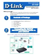
Express Ethernetwork DI-704P
Brand: D-Link Pages: 17

BiPAC 4500NZ(L)
Brand: Billion Pages: 146

3C3FE574BT
Brand: 3Com Pages: 8

8 Port 10/100Mbit/s Ethernet Smart Switch with Fibre Uplink
Brand: Tyco Electronics Pages: 18

Q5
Brand: JCG Pages: 3

WS-650 lite Series
Brand: Laurell Pages: 84

Firebox SOHO 6 Wireless
Brand: Watchguard Pages: 8

DVW3201B
Brand: Ubee Pages: 9

EK-FC1080 GTX Ti TF6
Brand: ekwb Pages: 2

ADAU1961
Brand: Analog Devices Pages: 76

ION 1200 Series
Brand: PaloAlto Networks Pages: 90

RP614 v2
Brand: NETGEAR Pages: 2

Extreme Gaming VGA Cooler GV1000
Brand: ZALMAN Pages: 7

CEM820 Series
Brand: AXIOMTEK Pages: 58

QSW-2900
Brand: QTech Pages: 406

ZM80C-HP
Brand: ZALMAN Pages: 18

AT-AR3050S
Brand: Allied Telesis Pages: 80

H80i v2
Brand: Corsair Pages: 12


