CIS VISION:mini VCC-F22S29APCL, Product Specification & Operational Manual
Introducing CIS VISION:mini VCC-F22S29APCL, a versatile surveillance camera designed to meet your security needs. Our Product Specification & Operational Manual is available for free download, providing comprehensive guidance on setup and usage. Access this essential manual from manualshive.com, ensuring a seamless user experience with our innovative product.
Share
Download


Reviews:
No comments
Related manuals for VISION:mini VCC-F22S29APCL
ECO Series
Brand: Okina USA Pages: 2
SP-45001C-CXP2A
Brand: JAI Pages: 78
MKC-X800
Brand: Ikegami Pages: 91
AP-3200T-10GE
Brand: JAI Pages: 75
See3CAM CU40
Brand: e-con Systems Pages: 22

DF3000AXS
Brand: dallmeier Pages: 33

27X
Brand: D-MAX Pages: 38
DS-2CC1172P
Brand: HIKVISION Pages: 97
SK-HD1800
Brand: Hitachi Pages: 90
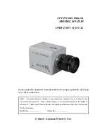
HV-D30
Brand: Hitachi Pages: 65
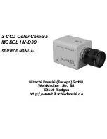
HV-D30
Brand: Hitachi Pages: 60
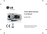
L5213R-BN
Brand: LG Pages: 2
LSX701
Brand: LG Pages: 42

Spy Camera Pen
Brand: Spycrushers Pages: 10
CCBS1345-LP
Brand: Siemens Pages: 6
FCB-CV7320
Brand: Sony Pages: 70

FCB-CV7520
Brand: Sony Pages: 71
HDC-900 Series
Brand: Sony Pages: 203


