background image

Preliminary Product Information

This document contains information for a new product.
Cirrus Logic reserves the right to modify this product without notice.

Copyright 

©

 Cirrus Logic, Inc. 2005

(All Rights Reserved)

Cirrus Logic, Inc.

http://www.cirrus.com

CS42528

114 dB, 192 kHz 8-Ch Codec with S/PDIF Receiver

Features

z

Eight 24-bit D/A, two 24-bit A/D Converters

z

114 dB DAC / 114 dB ADC Dynamic Range

z

-100 dB THD+N

z

System Sampling Rates up to 192 kHz

z

S/PDIF Receiver Compatible with EIAJ CP1201 

and IEC-60958

z

Recovered S/PDIF Clock or System Clock 

Selection

z

8:2 S/PDIF Input MUX

z

ADC High-pass Filter for DC Offset Calibration

z

Expandable ADC Channels and One-line Mode 

Support

z

Digital Output Volume Control with Soft Ramp

z

D/-15dB Input Gain Adjust for ADC

z

Differential Analog Architecture

z

Supports logic levels between 5 V and 1.8 V.

General Description

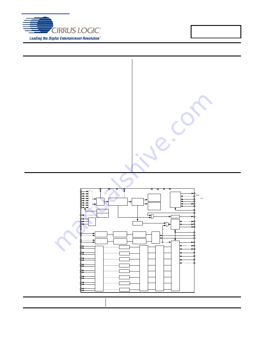
The CS42528 codec provides two analog-to-digital and eight
digital-to-analog delta-sigma converters, as well as an integrat-
ed S/PDIF receiver, in a 64-pin LQFP package.

The CS42528 integrated S/PDIF receiver supports up to eight
inputs, clock recovery circuitry and format auto-detection. The
internal stereo ADC is capable of independent channel gain
control for single-ended or differential analog inputs. All eight
channels of DAC provide digital volume control and differential
analog outputs. The general purpose outputs may be driven
high or low, or mapped to a variety of DAC mute controls or
ADC overflow indicators.

The CS42528 is ideal for audio systems requiring wide dynam-
ic range, negligible distortion and low noise, such as A/V
receivers, DVD receivers, digital speaker and automotive audio
systems.

ORDERING INFORMATION

CS42528-CQZ

-10° to 70° C

64-pin LQFP

Lead Free

CS42528-DQZ

-40° to 85° C

64-pin LQFP

Lead Free

CDB42528

Evaluation Board


RST

RXP0

RXP1/G PO 1

AD0/CS

SCL/CCLK

SDA/C DO UT

AD 1/C DIN

VLC

AO UT A1+
AO UT A1-

AO U TB1+

AO U TA3+
AO UT A3-

AO UT A2-

AO U TB2-

AO U TA2+

AO UT B2+

AO UTB1-

AO U TB3+
AO UTB3-

AO UT A4+
AO U TA4-

AO UT B4+
AO UT B4-

AINL+

AINL-

AIN R+

AINR -

F ILT+

REFG ND

VQ

Ref

ADC#1

ADC #2

Digital Filter

Digital Filter

G ain & C lip

G ain & Clip

CX_SDO UT

AD CIN1

ADC IN2

CX_SCLK

CX_LRC K

CX_SDIN4

CX_SD IN 3

CX_SDIN2

CX_SDIN1

VLS

SAI_LRC K

SAI_SCLK

SAI_SDO UT

D G ND

VD

O M CK

RM CK

LPF LT

T XP

IN T

Rx

Clock/D ata

Recovery

S/PDIF

Decoder

DEM

Serial
Audio

Interface

Port

C&U Bit

Data Buffer

Control

Port

DAC #1

D AC #2

DAC#3

D AC #4

DAC#5

DAC#6

DAC#7

DAC #8

D

ig

it

a

F

il

te

r

V

o

lu

m

e

 C

o

n

tr

o

l

DG N D

RXP2/G PO 2
RXP3/G PO 3
RXP4/G PO 4
RXP5/G PO 5
RXP6/G PO 6
RXP7/G PO 7

VD

M UTEC

G PO

M UTE

A

n

a

lo

g

 F

il

te

r

VARX

AG ND

ADC

Serial

Data

AG ND

VA

Internal M CLK

CO D EC

Serial

Port

M ult/Div

F orm at

Detector

JAN ‘05

DS586PP5

查询CDB42528供应商

查询CDB42528供应商

Summary of Contents for CDB42528

Page 1: ... control for single ended or differential analog inputs All eight channels of DAC provide digital volume control and differential analog outputs The general purpose outputs may be driven high or low or mapped to a variety of DAC mute controls or ADC overflow indicators The CS42528 is ideal for audio systems requiring wide dynam ic range negligible distortion and low noise such as A V receivers DVD...

Page 2: ...iltering 22 4 3 2 Interpolation Filter 22 4 3 3 Digital Volume and Mute Control 23 4 3 4 ATAPI Specification 23 4 4 S PDIF Receiver 24 4 4 1 8 2 S PDIF Input Multiplexer 24 4 4 2 Error Reporting and Hold Function 24 4 4 3 Channel Status Data Handling 24 4 4 4 User Data Handling 24 4 4 5 Non Audio Auto Detection 24 4 5 Clock Generation 25 4 5 1 PLL and Jitter Attenuation 25 4 5 2 OMCK System Clock ...

Page 3: ...e Control address 1Eh 62 6 19 Receiver Mode Control 2 address 1Fh 63 6 20 Interrupt Status address 20h Read Only 64 6 21 Interrupt Mask address 21h 65 6 22 Interrupt Mode MSB address 22h Interrupt Mode LSB address 23h 65 6 23 Channel Status Data Buffer Control address 24h 66 6 24 Receiver Channel Status address 25h Read Only 67 6 25 Receiver Errors address 26h Read Only 68 6 26 Receiver Errors Mas...

Page 4: ...l Audio Format 31 Figure 15 ADCIN1 ADCIN2 Serial Audio Format 32 Figure 16 OLM Configuration 1 33 Figure 17 OLM Configuration 2 34 Figure 18 OLM Configuration 3 35 Figure 19 OLM Configuration 4 36 Figure 20 OLM Configuration 5 37 Figure 21 Control Port Timing in SPI Mode 38 Figure 22 Control Port Timing I2 C Write 39 Figure 23 Control Port Timing I2 C Read 39 Figure 24 Recommended Analog Input Buf...

Page 5: ...3 Double Speed fast Stopband Rejection 87 Figure 54 Double Speed fast Transition Band 87 Figure 55 Double Speed fast Transition Band detail 87 Figure 56 Double Speed fast Passband Ripple 87 Figure 57 Double Speed slow Stopband Rejection 88 Figure 58 Double Speed slow Transition Band 88 Figure 59 Double Speed slow Transition Band detail 88 Figure 60 Double Speed slow Passband Ripple 88 Figure 61 Qu...

Page 6: ... Mode 51 Table 9 DAC One Line Mode 51 Table 10 RMCK Divider Settings 53 Table 11 OMCK Frequency Settings 54 Table 12 Master Clock Source Select 54 Table 13 AES Format Detection 55 Table 14 Receiver Clock Frequency Detection 56 Table 15 Example Digital Volume Settings 59 Table 16 ATAPI Decode 61 Table 17 Example ADC Input Gain Settings 62 Table 18 TXP Output Selection 63 Table 19 Receiver Input Sel...

Page 7: ...ins will not cause SCR latch up 2 The maximum over under voltage is limited by the input current Parameter Symbol Min Typ Max Units DC Power Supply Analog Digital Serial Port Interface Control Port Interface VA VARX VD VLS VLC 4 75 3 13 1 8 1 8 5 0 3 3 5 0 5 0 5 25 5 25 5 25 5 25 V V V V Ambient Operating Temperature power applied CS42528 CQZ CS42528 DQZ TA 10 40 70 85 C C Parameters Symbol Min Ma...

Page 8: ...c Range A weighted unweighted 40 kHz bandwidth unweighted 108 105 114 111 108 106 103 114 111 108 dB dB dB Total Harmonic Distortion Noise Note 3 1 dB 20 dB 60 dB 40 kHz bandwidth 1 dB THD N 100 91 51 97 94 100 91 51 97 92 dB dB dB dB Quad Speed Mode Fs 192 kHz Dynamic Range A weighted unweighted 40 kHz bandwidth unweighted 108 105 114 111 108 106 103 114 111 108 dB dB dB Total Harmonic Distortion...

Page 9: ... 0 µs Double Speed Mode 50 to 100 kHz sample rates Passband 0 1 dB Note 5 0 0 45 Fs Passband Ripple 0 035 dB Stopband Note 5 0 68 Fs Stopband Attenuation 92 dB Total Group Delay Fs Output Sample Rate tgd 9 Fs s Group Delay Variation vs Frequency tgd 0 0 µs Quad Speed Mode 100 to 192 kHz sample rates Passband 0 1 dB Note 5 0 0 24 Fs Passband Ripple 0 035 dB Stopband Note 5 0 78 Fs Stopband Attenuat...

Page 10: ... CS42528 DQZ Min Typ Max Unit Dynamic performance for all modes Dynamic Range Note 7 24 bit A Weighted unweighted 16 bit A Weighted Note 8 unweighted 108 105 114 111 97 94 106 103 114 111 97 94 dB dB dB dB Total Harmonic Distortion Noise 24 bit 0 dB 20 dB 60 dB 16 bit 0 dB Note 8 20 dB 60 dB THD N 100 91 51 94 74 34 94 100 91 51 94 74 34 92 dB dB dB dB dB dB Idle Channel Noise Signal to noise rati...

Page 11: ...Attenuation Note 10 90 64 dB Group Delay 12 Fs 6 5 Fs s Passband Group Delay Deviation 0 20 kHz 0 41 Fs 0 14 Fs s De emphasis Error Note 11 Fs 32 kHz Relative to 1 kHz Fs 44 1 kHz Fs 48 kHz 0 23 0 14 0 09 0 23 0 14 0 09 dB dB dB Combined Digital and On chip Analog Filter Response Double Speed Mode 96 kHz Passband Note 9 to 0 01 dB corner to 3 dB corner 0 0 0 4166 0 4998 0 0 0 2083 0 4998 Fs Fs Fre...

Page 12: ...uency Note 13 1 024 25 600 MHz OMCK Duty Cycle Note 13 40 50 60 CX_SCLK SAI_SCLK Duty Cycle 45 50 55 CX_LRCK SAI_LRCK Duty Cycle 45 50 55 Master Mode RMCK to CX_SCLK SAI_SCLK active edge delay tsmd 0 15 ns RMCK to CX_LRCK SAI_LRCK delay tlmd 0 15 ns Slave Mode CX_SCLK SAI_SCLK Falling Edge to CX_SDOUT SAI_SDOUT Output Valid tdpd 50 ns CX_LRCK SAI_LRCK Edge to MSB Valid tlrpd 20 ns CX_SDIN Setup Ti...

Page 13: ...to Start tirs 500 ns Bus Free Time Between Transmissions tbuf 4 7 µs Start Condition Hold Time prior to first clock pulse thdst 4 0 µs Clock Low time tlow 4 7 µs Clock High Time thigh 4 0 µs Setup Time for Repeated Start Condition tsust 4 7 µs SDA Hold Time from SCL Falling Note 16 thdd 0 µs SDA Setup time to SCL Rising tsud 250 ns Rise Time of SCL and SDA trc 1 µs Fall Time SCL and SDA tfc 300 ns...

Page 14: ...han or equal to 1 024 MHz should be safe for all possible conditions 20 Data must be held for sufficient time to bridge the transition time of CCLK 21 For fsck 1 MHz Parameter Symbol Min Typ Max Units CCLK Clock Frequency Note 19 fsck 0 6 0 MHz CS High Time Between Transmissions tcsh 1 0 µs CS Falling to CCLK Edge tcss 20 ns CCLK Low Time tscl 66 ns CCLK High Time tsch 66 ns CDIN to CCLK Rising Se...

Page 15: ...as shown in Figure 5 Parameter Symbol Min Typ Max Units Power Supply Current normal operation VA VARX 5 V Note 22 VD 5 V VD 3 3 V Interface current VLC 5 V Note 23 VLS 5 V power down state all supplies Note 24 IA ID ID ILC ILS Ipd 75 85 51 250 13 250 mA mA mA µA mA µA Power Consumption Note 22 VA VARX 5 V VD VLS VLC 3 3 V normal operation power down Note 24 VA VARX 5 V VD VLS VLC 5 V normal operat...

Page 16: ...imit the loading on the signal to 1 CMOS load Parameters Note 26 Symbol Min Typ Max Units High Level Input Voltage Serial Port Control Port VIH 0 7xVLS 0 7xVLC V V Low Level Input Voltage Serial Port Control Port VIL 0 2xVLS 0 2xVLC V V High Level Output Voltage at Io 2 mA Note 27 Serial Port Control Port MUTEC GPOx TXP VOH VLS 1 0 VLC 1 0 VA 1 0 VD 1 0 V V V V Low Level Output Voltage at Io 2 mA ...

Page 17: ...Diagram SDA CDOUT 8 Serial Control Data Input Output SDA is a data I O line in I2 C mode and requires an external pull up resistor to the logic interface voltage as shown in the Typical Connection Diagram CDOUT is the output data line for the control port interface in SPI mode AD1 CDIN 9 Address Bit 1 I2 C Serial Control Data SPI Input AD1 is a chip address pin in I2 C mode CDIN is the input data ...

Page 18: ...dance state as long as the part is in power down mode The Mute Control pin goes to the selected active state during reset muting or if the master clock to left right clock frequency ratio is incorrect This pin is intended to be used as a control for external mute circuits to prevent the clicks and pops that can occur in any single supply system The use of external mute circuits are not manda tory ...

Page 19: ...of six channels on one serial data output line when the CS42528 is placed in One Line mode OMCK 59 External Reference Clock Input External clock reference that must be within the ranges specified in the register OMCK Frequency OMCK Freqx on page 54 SAI_LRCK 60 Serial Audio Interface Left Right Clock Input Output Determines which channel Left or Right is currently active on the serial audio data li...

Page 20: ...r 56 CX_SDOUT 54 SAI_SDOUT 48 46 49 44 45 47 RXP0 RXP1 GPO1 S PDIF Interface 50 TXP Driver Up to 8 Sources 43 RXP2 GPO2 RXP3 GPO3 RXP4 GPO4 RXP5 GPO5 RXP6 GPO6 RXP7 GPO7 42 OSC Analog Output Buffer 2 and Mute Circuit optional Analog Output Buffer 2 and Mute Circuit optional Analog Output Buffer 2 and M ute Circuit optional Analog Output Buffer 2 and Mute Circuit optional Analog Output Buffer 2 and...

Page 21: ...put sample rates up to 100 kHz and uses an oversampling ratio of 64x Quad Speed mode QSM supports input sample rates up to 192 kHz and uses an oversampling ratio of 32x Using the receiver clock recovery PLL a low jitter clock is recovered from the incoming S PDIF data stream The recovered clock or an externally supplied clock attached to the OMCK pin can be used as the System Clock 4 2 Analog Inpu...

Page 22: ...uiescent DC level of approximately VQ The delta sigma conversion process produces high frequency noise beyond the audio passband most of which is removed by the on chip analog filters The remaining out of band noise can be attenuated using an off chip low pass filter See DAC Output Filter on page 76 for a recommended output buffer This filter configuration accounts for the normally differing AC lo...

Page 23: ...wer down mode by setting the PDN bit in the register Power Control address 02h on page 48 to a 1 Once out of power down mode the pin can be con trolled by the user via the control port or automatically asserted high when zero data is present on all DAC inputs or when serial port clock errors are present To prevent large transients on the output it is desirable to mute the DAC outputs before the Mu...

Page 24: ...multiplexer defaults to RXP0 for both functions 4 4 2 Error Reporting and Hold Function While decoding the incoming S PDIF data stream the CS42528 can identify several kinds of error indi cated in the register Receiver Errors address 26h Read Only on page 68 See Error Reporting and Hold Function on page 77 for more information 4 4 3 Channel Status Data Handling The first 2 bytes of the Channel Sta...

Page 25: ... generate the required internal master clock frequency By setting the PLL_LRCK bit to a 1 in the register Clock Control address 06h on page 53 the PLL will lock to the incoming SAI_LRCK and generate an output master clock RMCK of 256Fs Table 2 shows the output of the PLL with typical input Fs values for SAI_LRCK See Appendix C PLL Filter on page 80 for more information concerning PLL operation req...

Page 26: ...dress 06h on page 53 The supported PLL output frequencies are shown in Table 2 below 4 5 4 Slave Mode In Slave mode CX_LRCK CX_SCLK and or SAI_LRCK SAI_SCLK operate as inputs The Left Right clock signal must be equal to the sample rate Fs and must be synchronously derived from the supplied master clock OMCK or the output of the PLL The serial bit clock CX_SCLK and or SAI_SCLK must be synchronously...

Page 27: ...EC_SP to be different but must be multiples of each other The serial data interface format selection left right justified I2 S or one line mode for the Serial Audio In terface serial port data out pin SAI_SDOUT the CODEC serial port data out pin CX_SDOUT and the CODEC input pins CX_SDIN1 4 is configured using the appropriate bits in the register Interface For mats address 04h on page 50 The serial...

Page 28: ...ADC 1 ADC 2 ADC channels 1 2 3 4 5 6 SAI_SDOUT left channel right channel one line mode S PDIF Left or ADC 1 S PDIF Right or ADC 2 ADC channels 1 2 3 4 5 6 ADCIN1 left channel right channel External ADC 3 External ADC 4 ADCIN2 left channel right channel External ADC 5 External ADC 6 Serial Inputs Outputs Table 4 Serial Audio Port Channel Allocations ...

Page 29: ...equivalent to Fs 32 44 1 48 kHz double speed mode is for Fs 64 88 2 96 kHz and quad speed mode is for Fs 176 4 196 kHz Left Channel Right Channel CX_SDINx CX_SDOUT SAI_SDOUT 3 2 1 5 4 1 2 3 4 5 3 2 1 5 4 1 2 3 4 MSB MSB LSB LSB CX_LRCK SAI_LRCK CX_SCLK SAI_SCLK Figure 10 I2 S Serial Audio Formats I2S Mode Data Valid on Rising Edge of SCLK Bits Sample SCLK Rate s Notes Master Slave 16 64 48 64 128 ...

Page 30: ...256 Fs 48 64 128 Fs single speed mode 64 Fs 48 64 Fs double speed mode 64 Fs 48 64 Fs quad speed mode Left Channel Right Channel 6 5 4 3 2 1 0 9 8 7 15 14 13 12 11 10 6 5 4 3 2 1 0 9 8 7 15 14 13 12 11 10 CX_SDINx CX_SDOUT SAI_SDOUT CX_LRCK SAI_LRCK CX_SCLK SAI_SCLK Figure 12 Right Justified Serial Audio Formats Right Justified Mode Data Valid on Rising Edge of SCLK Bits Sample SCLK Rate s Notes M...

Page 31: ...C7 DAC8 20 clks CX_SDIN4 20 clks ADC1 ADC3 ADC5 ADC2 ADC4 ADC6 20 clks 20 clks 20 clks 20 clks 20 clks CX_SDOUT SAI_SDOUT CX_SDIN1 LSB MSB 24clks 128clks LSB MSB LSB MSB LSB MSB LSB MSB LSB MSB MSB DAC1 DAC3 DAC5 DAC2 DAC4 DAC6 24clks 24clks 24clks 24clks 24clks Left Channel Right Channel 24clks DAC7 DAC8 24clks 24clks ADC1 ADC3 ADC5 ADC2 ADC4 ADC6 24clks 24clks 24clks 24clks 24clks 128clks CX_LRC...

Page 32: ...eration the CS42528 must be configured to select which SCLK LRCK is being used to clock the external ADCs The EXT ADC SCLK bit in register Misc Control address 05h on page 52 must be set accordingly Set this bit to 1 if the external ADCs are wired using the CODEC_SP clocks If the ADCs are wired to use the SAI_SP clocks set this bit to 0 CX_LRCK SAI_LRCK CX_SCLK SAI_SCLK Left Channel Right Channel ...

Page 33: ...r addr 05h Set CODEC_SP M S 1 Configure CODEC Serial Port to master mode Set SAI_SP M S 1 Configure Serial Audio Interface Port to master mode Set EXT ADC SCLK 0 Identify external ADC clock source as SAI Serial Port DAC Mode Not One Line Mode One Line Mode 1 One Line Mode 2 ADC Mode Not One Line Mode CX_SCLK 64 Fs CX_LRCK SSM DSM QSM SAI_SCLK 64 Fs SAI_LRCK CX_LRCK CX_SCLK 128 Fs CX_LRCK SSM DSM S...

Page 34: ...g mode see table below for valid combinations Misc Control Register addr 05h Set CODEC_SP M S 1 Set CODEC Serial Port to master mode Set SAI_SP M S 1 Set Serial Audio Interface Port to master mode Set EXT ADC SCLK 1 Identify external ADC clock source as CODEC Serial Port CX_SDOUT not used SAI_SDOUT ADC Data DAC Mode Not One Line Mode One Line Mode 1 One Line Mode 2 ADC Mode Not One Line Mode CX_SC...

Page 35: ...lid combinations Set DAC_OLx bits 00 01 Select DAC operating mode see table below for valid combinations Misc Control Register addr 05h Set CODEC_SP M S 1 Set CODEC Serial Port to master mode Set SAI_SP M S 0 or 1 Set Serial Audio Interface Port to master mode or slave mode Set EXT ADC SCLK 1 Identify external ADC clock source as CODEC Serial Port CX_SDOUT ADC Data SAI_SDOUT S PDIF Data DAC Mode N...

Page 36: ...lid combinations Set DAC_OLx bits 00 01 10 Select DAC operating mode see table below for valid combinations Misc Control Register addr 05h Set CODEC_SP M S 1 Set DAC Serial Port to master mode Set SAI_SP M S 0 or 1 Set ADC Serial Port to master mode or slave mode Set EXT ADC SCLK 0 Identify external ADC clock source as SAI Serial Port CX_SDOUT not used SAI_SDOUT ADC Data DAC Mode Not One Line Mode...

Page 37: ...de Set ADC_OLx bits 00 Set ADC operating mode to Not One Line Mode since only 2 channels of ADC are supported Set DAC_OLx bits 00 01 Select DAC operating mode see table below for valid combinations Misc Control Register addr 05h Set CODEC_SP M S 0 or 1 Set CODEC Serial Port to master mode or slave mode Set SAI_SP M S 0 or 1 Set Serial Audio Interface Port to master mode or slave mode Set EXT ADC S...

Page 38: ...bit is a read write indi cator R W which should be low to write The next eight bits form the Memory Address Pointer MAP which is set to the address of the register that is to be updated The next eight bits are the data which will be placed into the register designated by the MAP During writes the CDOUT output stays in the Hi Z state It may be externally pulled high or low with a 47 kΩ resistor if ...

Page 39: ...f the op eration is a read the contents of the register pointed to by the MAP will be output Setting the auto incre ment bit in MAP allows successive reads or writes of consecutive registers Each byte is separated by an acknowledge bit The ACK bit is output from the CS42528 after each input byte is read and is input to the CS42528 from the microcontroller after each transmitted byte Since the read...

Page 40: ...ternal states are reset including the control port and registers and the outputs are muted When RST is high the control port becomes oper ational and the desired settings should be loaded into the control registers Writing a 0 to the PDN bit in the Power Control Register will then cause the part to leave the low power state and begin operation If the internal PLL is selected as the clock source th...

Page 41: ...st to the pin and should be mounted on the same side of the board as the CS42528 to minimize inductance effects All signals especially clocks should be kept away from the FILT VQ and LPFLT pins in order to avoid unwanted coupling into the modulators and PLL The FILT and VQ decoupling capacitors particularly the 0 1 µF must be positioned to minimize the electrical path from FILT and REFGND The CDB4...

Page 42: ...1 RMCK_DIV0 OMCK Freq1 OMCK Freq0 PLL_LRCK SW_CTRL1 SW_CTRL0 FRC_PLL_LK page 53 default 0 0 0 0 0 0 0 0 07h OMCK PLL_ CLK Ratio RATIO7 RATIO6 RATIO5 RATIO4 RATIO3 RATIO2 RATIO1 RATIO0 page 55 default X X X X X X X X 08h RVCR Sta tus Digital Silence AES Format2 AES Format1 AES Format0 Active_CLK RVCR_CLK2 RVCR_CLK1 RVCR_CLK0 page 55 default X X X X X X X X 09h Burst Pre amble PC Byte 0 PC0 7 PC0 6 ...

Page 43: ...VOL4 B3_VOL3 B3_VOL2 B3_VOL1 B3_VOL0 page 59 default 0 0 0 0 0 0 0 0 15h Vol Control A4 A4_VOL7 A4_VOL6 A4_VOL5 A4_VOL4 A4_VOL3 A4_VOL2 A4_VOL1 A4_VOL0 page 59 default 0 0 0 0 0 0 0 0 16h Vol Control B4 B4_VOL7 B4_VOL6 B4_VOL5 B4_VOL4 B4_VOL3 B4_VOL2 B4_VOL1 B4_VOL0 page 59 default 0 0 0 0 0 0 0 0 17h Channel Invert INV_B4 INV_A4 INV_B3 INV_A3 INV_B2 INV_A2 INV_B1 INV_A1 page 59 default 0 0 0 0 0 ...

Page 44: ...Interrupt Mode MSB UNLOCK1 Reserved QCH1 DETC1 DETU1 Reserved OF1 RERR1 page 65 default 0 0 0 0 0 0 0 0 23h Interrupt Mode LSB UNLOCK0 Reserved QCH0 DETC0 DETU0 Reserved OF0 RERR0 page 65 default 0 0 0 0 0 0 0 0 24h Buffer Ctrl Reserved LOCKM Reserved Reserved Reserved BSEL CAM CHS page 66 default 0 1 0 0 0 0 0 0 25h RCVR CS Data AUX3 AUX2 AUX1 AUX0 PRO AUDIO COPY ORIG page 67 default 0 0 0 0 0 0 ...

Page 45: ...X X X X X X X 31h Q Subcode Track7 Track6 Track5 Track4 Track3 Track2 Track1 Track0 page 72 default X X X X X X X X 32h Q Subcode Index7 Index6 Index5 Index4 Index3 Index2 Index1 Index0 page 72 default X X X X X X X X 33h Q Subcode Minute7 Minute6 Minute5 Minute4 Minute3 Minute2 Minute1 Minute0 page 72 default X X X X X X X X 34h Q Subcode Second7 Second6 Second5 Second4 Second3 Second2 Second1 Se...

Page 46: ...CS42528 46 DS586PP5 3Ah C or U Data Buffer CU Buffer7 CU Buffer6 CU Buffer5 CU Buffer4 CU Buffer3 CU Buffer2 CU Buffer1 CU Buffer0 51h page 72 default X X X X X X X X Addr Function 7 6 5 4 3 2 1 0 ...

Page 47: ...pointer auto increment control 0 MAP is not incremented automatically 1 Internal MAP is automatically incremented after each read or write 6 1 2 MEMORY ADDRESS POINTER MAPX Default 0000001 Function Memory address pointer MAP Sets the register address that will be read or written by the control port 6 2 Chip I D and Revision Register address 01h Read Only 6 2 1 CHIP I D CHIP_IDX Default 1111 Functi...

Page 48: ...with the PDN_RCVR0 bit 6 3 2 POWER DOWN ADC PDN_ADC Default 0 Function When enabled the stereo analog to digital converter will remain in a reset state It is advised that any change of this bit be made while the DACs are muted or the power down bit PDN is enabled to elim inate the possibility of audible artifacts 6 3 3 POWER DOWN DAC PAIRS PDN_DACX Default 0 Function When enabled the respective DA...

Page 49: ...rresponding sample rate range when the SAI_SP is in Master or Slave mode 6 4 3 ADC SERIAL PORT SELECT ADC_SP SELX Default 00 00 Serial data on CX_SDOUT pin clocked from the CODEC_SP S PDIF data on SAI_SDOUT pin 01 Serial data on CX_SDOUT pin clocked from the SAI_SP S PDIF data on SAI_SDOUT pin 10 Serial data on SAI_SDOUT pin clocked from the SAI_SP No S PDIF data available 11 Reserved Function Sel...

Page 50: ...ate sample rate 6 5 Interface Formats address 04h 6 5 1 DIGITAL INTERFACE FORMAT DIFX Default 01 Function These bits select the digital interface format used for the CODEC Serial Port and Serial Audio Interface Port when not in one_line mode The required relationship between the Left Right clock serial clock and serial data is defined by the Digital Interface Format and the options are detailed in...

Page 51: ... SAI_RJ16 Default 0 Function This bit determines how many bits to use during right justified mode for the Serial Audio Interface Port By default the receiver will be in RJ24 bits but can be set to RJ16 bits 0 24 bit mode 1 16 bit mode DIF1 DIF0 Description Format Figure 0 0 Left Justified up to 24 bit data 0 11 0 1 I2 S up to 24 bit data 1 10 1 0 Right Justified 16 bit or 24 bit data 2 12 1 1 rese...

Page 52: ...output on RMCK when the clock signal is not required 6 6 3 FREEZE CONTROLS FREEZE Default 0 Function This function will freeze the previous output of and allow modifications to be made to the Volume Control address 0Fh 16h Channel Invert address 17h and Mixing Control Pair address 18h 1Bh registers without the changes taking effect until the FREEZE is disabled To make multiple changes in these con...

Page 53: ...is in slave mode then CX_LRCK and CX_SCLK must be present 6 6 7 SERIAL AUDIO INTERFACE SERIAL PORT MASTER SLAVE SELECT SAI_SP M S Default 0 Function In Master mode SAI_SCLK and SAI_LRCK are outputs Internal dividers will divide the master clock to generate the serial clock and left right clock In Slave mode SAI_SCLK and SAI_LRCK become inputs If the internal MCLK is sourced from the output of the ...

Page 54: ... the FRC_PLL_LK bit is set to 1 b then RMCK will not equal OMCK 6 7 5 FORCE PLL LOCK FRC_PLL_LK Default 0 Function This bit is used to enable the PLL to lock to the S PDIF input stream or the SAI_LRCK with the ab sence of a clock signal on OMCK When set to a 1 b the auto detect sample frequency feature will be disabled and the SW_CTRLX bits must be set to 00 b The OMCK PLL_CLK Ratio address 07h Re...

Page 55: ...e detected Function The CS42528 will auto detect a digital silence condition when 1548 consecutive zeros have been de tected 6 9 2 AES FORMAT DETECTION AES FORMATX Default xxx Function The CS42528 will auto detect the AES format of the incoming S PDIF stream and display the infor mation according to the following table 7 6 5 4 3 2 1 0 RATIO7 21 RATIO6 20 RATIO5 2 1 RATIO4 2 2 RATIO3 2 3 RATIO2 2 4...

Page 56: ...re quency of the PLL clock does not match one of the given frequencies this register will display the closest available value NOTE These bits are set to 111 b when the FRC_PLL_LK bit is 1 b 6 10 Burst Preamble PC and PD Bytes addresses 09h 0Ch Read Only 6 10 1 BURST PREAMBLE BITS PCX PDX Default xxh Function The PC and PD burst preamble bytes are loaded into these four registers RCVR_CLK2 RCVR_CLK...

Page 57: ... requested level change will occur after a timeout period between 512 and 1024 sample periods 10 7 ms to 21 3 ms at 48 kHz sample rate if the signal does not encounter a zero crossing The zero cross function is independently mon itored and implemented for each channel Soft Ramp Soft Ramp allows level changes both muting and attenuation to be implemented by incrementally ramping in 1 8 dB steps fro...

Page 58: ...ault 0 0 Disabled 1 Enabled Function An un mute will be performed after executing a filter mode change after a MCLK LRCK ratio change or error and after changing the Functional Mode When this feature is enabled this un mute is affect ed similar to attenuation changes by the Soft and Zero Cross bits SZC 1 0 When disabled an im mediate un mute is performed in these instances Note For best results it...

Page 59: ...are decoded as shown in Table 15 The volume changes are implemented as dictated by the Soft and Zero Cross bits SZC 1 0 All volume settings less than 127 dB are equivalent to enabling the MUTE bit for the given channel 6 14 Channel Invert address 17h 6 14 1 INVERT SIGNAL POLARITY INV_XX Default 0 0 Disabled 1 Enabled Function When enabled these bits will invert the signal polarity of their respect...

Page 60: ...Default 0 0 Disabled 1 Enabled Function The AOUTAx and AOUTBx volume levels are independently controlled by the A and the B Channel Volume Control registers when this function is disabled The volume on both AOUTAx and AOUTBx are determined by the A Channel Volume Control registers per A B pair and the B Channel Volume Control registers are ignored when this function is enabled 7 6 5 4 3 2 1 0 Px_A...

Page 61: ... 0 0 1 1 MUTE b L R 2 0 0 1 0 0 aR MUTE 0 0 1 0 1 aR bR 0 0 1 1 0 aR bL 0 0 1 1 1 aR b L R 2 0 1 0 0 0 aL MUTE 0 1 0 0 1 aL bR 0 1 0 1 0 aL bL 0 1 0 1 1 aL b L R 2 0 1 1 0 0 a L R 2 MUTE 0 1 1 0 1 a L R 2 bR 0 1 1 1 0 a L R 2 bL 0 1 1 1 1 a L R 2 b L R 2 1 0 0 0 0 MUTE MUTE 1 0 0 0 1 MUTE bR 1 0 0 1 0 MUTE bL 1 0 0 1 1 MUTE aL bR 2 1 0 1 0 0 aR MUTE 1 0 1 0 1 aR bR 1 0 1 1 0 aR bL 1 0 1 1 1 aR bL ...

Page 62: ...ble 17 6 18 Receiver Mode Control address 1Eh 6 18 1 SERIAL PORT SYNCHRONIZATION SP_SYNC Default 0 0 CX SAI Serial Port timings not in phase 1 CX SAI Serial Port timings are in phase Function Forces the LRCK and SCLK from the CX SAI Serial Ports to align and operate in phase This func tion will operate when both ports are running at the same sample rate or when operating at different sample rates ...

Page 63: ...nes how the interrupt pin INT will indicate an interrupt condition 6 18 4 AUDIO SAMPLE HOLD HOLDX Default 00 00 Hold the last valid audio sample 01 Replace the current audio sample with 00 mute 10 Do not change the received audio sample 11 Reserved Function Determines how received audio samples are affected when a receiver error occurs 6 19 Receiver Mode Control 2 address 1Fh 6 19 1 TXP MULTIPLEXE...

Page 64: ...r 6 20 1 PLL UNLOCK UNLOCK Default 0 Function PLL unlock status bit This bit will go high if the PLL becomes unlocked 6 20 2 NEW Q SUBCODE BLOCK QCH Default 0 Function Indicates when the Q Subcode block has changed 6 20 3 D TO E C BUFFER TRANSFER DETC Default 0 Function Indicates when the channel status buffer has changed 1 1 0 Output from pin RXP6 1 1 1 Output from pin RXP7 RMUX2 RMUX1 RMUX0 Desc...

Page 65: ...rrence will not affect the INT pin or the status register The bit positions align with the corresponding bits in the Interrupt Status register 6 22 Interrupt Mode MSB address 22h Interrupt Mode LSB address 23h Default 00000000 Function The two Interrupt Mode registers form a 2 bit code for each Interrupt Status register function There are three ways to set the INT pin active in accordance with the...

Page 66: ...tatus data 1 Data buffer address space contains User data Function Selects the data buffer register addresses to contain either User data or Channel Status data 6 23 3 C DATA BUFFER CONTROL CAM Default 0 0 One byte mode 1 Two byte mode Function Sets the C data buffer control port access mode 6 23 4 CHANNEL SELECT CHS Default 0 Function When set to 0 channel A information is displayed in the receiv...

Page 67: ...he received data is not linearly coded PCM audio 6 24 4 SCMS COPYRIGHT COPY Default x Function A 0 indicates that copyright is not asserted while a 1 indicates that copyright is asserted If the cat egory code is set to General in the incoming S PDIF digital stream copyright will always be indicated by COPY even when the stream indicates no copyright 6 24 5 SCMS GENERATION ORIG Default x 7 6 5 4 3 ...

Page 68: ...ion Indicates a channel status block cyclic redundancy This bit is updated on CS block boundaries valid in Professional mode 6 25 3 PLL LOCK STATUS UNLOCK Default x 0 PLL locked 1 PLL out of lock Function Indicates the lock status of the PLL 6 25 4 RECEIVED VALIDITY V Default x 0 Data is valid and is normally linear coded PCM audio 1 Data is invalid or may be valid compressed audio Function Indica...

Page 69: ...ccurrence will appear in the receiver errors register will affect the RERR interrupt and will affect the current audio sample according to the status of the HOLD bit If a mask bit is set to 0 the error is masked meaning that its occurrence will not appear in the receiver error register will not affect the RERR interrupt and will not affect the cur rent audio sample The CCRC and QCRC bits behave di...

Page 70: ... output driven low or as a dedicated ADC overflow pin indicating an over range condition anywhere in the ADC signal path for either the left or right channel The Functionx bits determine the operation of the pin When configured as a GPO with the output driven low the driver is a CMOS driver When configured to iden tify an ADC Overflow condition the driver is an open drain driver requiring a pull u...

Page 71: ...ional bits be set to 0 GPO Drive High If the pin is configured as a general purpose output then the functional bits are ignored and the pin is driven high It is recommended that in this mode all the functional bits be set to 0 RXPx GPOx Reg Address Function4 Function3 Function2 Function1 Function0 RXP7 GPO7 pin 42 29h M_AOUTA1 M_AOUTB1 M_AOUTA2 M_AOUTB2 M_AOUTA3 M_AOUTB3 M_AOUTA4 M_AOUTB4 RXP6 GPO...

Page 72: ...rack2 Track1 Track0 Index7 Index6 Index5 Index4 Index3 Index2 Index1 Index0 Minute7 Minute6 Minute5 Minute4 Minute3 Minute2 Minute1 Minute0 Second7 Second6 Second5 Second4 Second3 Second2 Second1 Second0 Frame7 Frame6 Frame5 Frame4 Frame3 Frame2 Frame1 Frame0 Zero7 Zero6 Zero5 Zero4 Zero3 Zero2 Zero1 Zero0 A Minute7 A Minute6 A Minute5 A Minute4 A Minute3 A Minute2 A Minute1 A Minute0 A Second7 A ...

Page 73: ...ther spectral components over the specified band width typically 10 Hz to 20 kHz including distortion components Expressed in decibels Measured at 1 and 20 dBFS as suggested in AES17 1991 Annex A Frequency Response A measure of the amplitude response variation from 10 Hz to 20 kHz relative to the amplitude response at 1 kHz Units in decibels Interchannel Isolation A measure of crosstalk between th...

Page 74: ...r for Digital Audio by D R Welland B P Del Signore E J Swanson T Tanaka K Hamashita S Hara K Takasuka Paper presented at the 85th Convention of the Audio Engineering Society November 1988 8 Cirrus Logic The Effects of Sampling Clock Jitter on Nyquist Sampling Analog to Digital Converters and on Oversampling Delta Sigma ADC s by Steven Harris Paper presented at the 87th Convention of the Audio Engi...

Page 75: ...0 398 9 90 10 0 BSC 10 10 E 0 461 0 472 BSC 0 484 11 70 12 0 BSC 12 30 E1 0 390 0 393 BSC 0 398 9 90 10 0 BSC 10 10 e 0 016 0 020 BSC 0 024 0 40 0 50 BSC 0 60 L 0 018 0 024 0 030 0 45 0 60 0 75 0 000 4 7 000 0 00 4 7 00 Nominal pin pitch is 0 50 mm Controlling dimension is mm JEDEC Designation MS026 Parameter Symbol Min Typ Max Units Allowable Junction Temperature 135 C Junction to Ambient Thermal...

Page 76: ...eramics must be avoided since these can degrade signal linearity 10 2 DAC Output Filter The CS42528 is a linear phase design and does not include phase or amplitude compensation for an ex ternal filter Therefore the DAC system phase and amplitude response will be dependent on the external analog circuitry VA 100 µF 100 kΩ 10 kΩ 3 32 kΩ 2 8 kΩ 0 1 µF 100 µF 470 pF 470 pF C0G C0G 634 Ω 634 Ω 634 Ω 9...

Page 77: ...el Status Data Handling The setting of the CHS bit in the register Channel Status Data Buffer Control address 24h on page 66 determines whether the channel status decodes are from the A channel CHS 0 or B channel CHS 1 The PRO professional bit is extracted directly For consumer data the COPY copyright bit is extracted and the category code and L bits are decoded to determine SCMS status indicated ...

Page 78: ...Register 11 2 1a One Byte mode In many applications the channel status blocks for the A and B channels will be identical In this situation the user may read a byte from one of the channel s blocks since the corresponding byte for the other chan nel will likely be the same One byte mode takes advantage of the often identical nature of A and B chan nel status data When reading data in one byte mode ...

Page 79: ...follows Bit15 A7 Bit14 B7 Bit13 A6 Bit12 B6 Bit1 A0 Bit0 B0 The arrangement of the data in each byte is as follows MSB is the first received bit and is the first trans mitted bit The first byte read is the first byte received and the first byte sent is the first byte transmitted When two bytes are read from the E buffer the bits are presented in the following arrangement A 7 B 7 A 6 B 6 A 0 B 0 11...

Page 80: ...ata dependent jitter effects because the S PDIF preambles do not vary with the data The PLL has the ability to lock onto a wide range of input sample rates with no external component chang es The nominal center sample rate is the sample rate that the PLL first locks onto upon application of an S PDIF data stream Phase Comparator and Charge Pump N VCO RMCK INPUT CRIP CFILT RFILT Figure 27 PLL Block...

Page 81: ...d that the ground end of the PLL filter be returned directly to the AGND pin independently of the digital ground plane It should be noted that for backward compatibility with Revision C these components may be used with Revision D silicon with the LOCKM register 24h bit 6 set to 0 12 1 2 Jitter Attenuation Shown in Figure 28 is the jitter attenuation plot when used with the external PLL component ...

Page 82: ... These include the Z5U and Y5V dielectrics 12 1 4 Circuit Board Layout Board layout and capacitor choice affect each other and determine the performance of the PLL Figure 29 illustrates a suggested layout for the PLL filter components and for bypassing the analog supply voltage The 10 µF bypass capacitor is an electrolytic in a surface mount case A or thru hole package RFILT CFILT CRIP and the 0 1...

Page 83: ... through a capacitor to chassis ground at the receiver However in some cases it is advantageous to have the ground of two boxes held at the same potential and make the electrical connection through the cable shield Generally it may be a good idea to provide the option of grounding or capacitively coupling the shield to the chassis When more than one RXP pin is driven simultaneously as shown in Fig...

Page 84: ...51 0 52 0 53 0 54 0 55 Frequency normalized to Fs Amplitude dB 0 10 0 08 0 05 0 03 0 00 0 03 0 05 0 08 0 10 0 00 0 05 0 10 0 15 0 20 0 25 0 30 0 35 0 40 0 45 0 50 Frequency normalized to Fs Amplitude dB Figure 35 Single Speed Mode Transition Band Detail Figure 36 Single Speed Mode Passband Ripple 140 130 120 110 100 90 80 70 60 50 40 30 20 10 0 0 0 0 1 0 2 0 3 0 4 0 5 0 6 0 7 0 8 0 9 1 0 Frequency...

Page 85: ... 0 6 0 7 0 8 0 9 1 0 Frequency normalized to Fs Amplitude dB 130 120 110 100 90 80 70 60 50 40 30 20 10 0 0 2 0 25 0 3 0 35 0 4 0 45 0 5 0 55 0 6 0 65 0 7 0 75 0 8 Frequency normalized to Fs Amplitude dB Figure 41 Quad Speed Mode Stopband Rejection Figure 42 Quad Speed Mode Transition Band 10 9 8 7 6 5 4 3 2 1 0 0 1 0 15 0 2 0 25 0 3 0 35 0 4 0 45 0 5 0 55 0 6 Frequency normalized to Fs Amplitude ...

Page 86: ...54 0 55 10 9 8 7 6 5 4 3 2 1 0 Frequency normalized to Fs Amplitude dB 0 0 05 0 1 0 15 0 2 0 25 0 3 0 35 0 4 0 45 0 5 0 02 0 015 0 01 0 005 0 0 005 0 01 0 015 0 02 Frequency normalized to Fs Amplitude dB Figure 47 Single Speed fast Transition Band detail Figure 48 Single Speed fast Passband Ripple 0 4 0 5 0 6 0 7 0 8 0 9 1 120 100 80 60 40 20 0 Frequency normalized to Fs Amplitude dB 0 4 0 42 0 44...

Page 87: ...0 60 40 20 0 Frequency normalized to Fs Amplitude dB 0 4 0 42 0 44 0 46 0 48 0 5 0 52 0 54 0 56 0 58 0 6 120 100 80 60 40 20 0 Frequency normalized to Fs Amplitude dB Figure 53 Double Speed fast Stopband Rejection Figure 54 Double Speed fast Transition Band 0 45 0 46 0 47 0 48 0 49 0 5 0 51 0 52 0 53 0 54 0 55 10 9 8 7 6 5 4 3 2 1 0 Frequency normalized to Fs Amplitude dB 0 0 05 0 1 0 15 0 2 0 25 ...

Page 88: ... 10 9 8 7 6 5 4 3 2 1 0 Frequency normalized to Fs Amplitude dB 0 0 05 0 1 0 15 0 2 0 25 0 3 0 35 0 02 0 015 0 01 0 005 0 0 005 0 01 0 015 0 02 Frequency normalized to Fs Amplitude dB Figure 59 Double Speed slow Transition Band detail Figure 60 Double Speed slow Passband Ripple 0 2 0 3 0 4 0 5 0 6 0 7 0 8 0 9 1 120 100 80 60 40 20 0 Frequency normalized to Fs Amplitude dB 0 2 0 3 0 4 0 5 0 6 0 7 0...

Page 89: ...120 100 80 60 40 20 0 Frequency normalized to Fs Amplitude dB 0 1 0 2 0 3 0 4 0 5 0 6 0 7 0 8 0 9 120 100 80 60 40 20 0 Frequency normalized to Fs Amplitude dB Figure 65 Quad Speed slow Stopband Rejection Figure 66 Quad Speed slow Transition Band 0 45 0 46 0 47 0 48 0 49 0 5 0 51 0 52 0 53 0 54 0 55 10 9 8 7 6 5 4 3 2 1 0 Frequency normalized to Fs Amplitude dB 0 0 02 0 04 0 06 0 08 0 1 0 12 0 02 ...

Page 90: ...ecifications in the Analog Output Characteristics table on page 10 Updated specification conditions for the analog input characteristics on page 8 Updated specification conditions for the analog output characteristics on page 10 Updated specification of tds and tdh in the Switching Characteristics table on page 12 Corrected reference to the SW_CTRL 1 0 bits in section 4 5 3 on page 26 Moved the VQ...

Page 91: ...ying such as copying for general distribution advertising or promotional purposes or for creating any work for resale CERTAIN APPLICATIONS USING SEMICONDUCTOR PRODUCTS MAY INVOLVE POTENTIAL RISKS OF DEATH PERSONAL INJURY OR SEVERE PROPERTY OR ENVIRONMENTAL DAMAGE CRITICAL APPLICATIONS CIRRUS PRODUCTS ARE NOT DESIGNED AUTHO RIZED OR WARRANTED FOR USE IN AIRCRAFT SYSTEMS MILITARY APPLICATIONS PRODUC...

Reviews: