background image


MI982 

Intel®  H81 Based Mini-ITX board 

Mini ITX Motherboard 


USER’S MANUAL 

Version 1.0


Summary of Contents for MI982

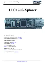
Page 1: ...MI982 Intel H81 Based Mini ITX board Mini ITX Motherboard USER S MANUAL Version 1 0 ...

Page 2: ...ess Machines Corporation Intel and Intel 4th Generation Core DC QC Processor are registered trademarks of Intel Corporation Microsoft Windows is a registered trademark of Microsoft Corporation Fintek is a registered trademark of Fintek Electronics Corporation All other product names or trademarks are properties of their respective owners ...

Page 3: ...he Jumpers 8 Connectors on MI982 14 BIOS Setup 28 Drivers Installation 54 Intel Chipset Software Installation Utility 55 VGA Drivers Installation 56 Realtek HD Audio Driver Installation 57 LAN Drivers Installation 58 Intel Management Engine Interface 59 Intel USB 3 0 Drivers 60 Appendix 62 A I O Port Address Map 62 B Interrupt Request Lines IRQ 63 C Watchdog Timer Configuration 64 ...

Page 4: ...iv MI982 User s Manual This page is intentionally left blank ...

Page 5: ...l 4th Gen Core DT processor integrated HD graphics supports 3 independent displays Direct X 11 1 OpenGL 3 2 and Open CL 1 2 Display interfaces are for HDMI DisplayPort and VGA CRT With two Gigabit Ethernets the MI982 Mini ITX board utilizes the dramatic increase in performance provided Intel s latest cutting edge technology Expansion is provided by PCIe 16x one full sized MiniPCIe and a half sized...

Page 6: ...layPort x 1 Thru port D VGA x 1 Thru PCH LAN 1 Intel I217LM PHY GbE 2 Intel I211AT PCIe GbE as 2nd LAN USB USB 2 0 host controller H81 Integrated support 8 ports 4 ports via the rear panel I O 2 ports via MiniPCIe socket 2 ports via pin header USB 3 0 host controller H81 Integrated support 2 ports 2 ports via the rear panel I O Serial ATA Intel H81 PCH built in SATA controller support 4 ports 2 x ...

Page 7: ...or 2 ports x SATA III Blue color 2 ports x SATA II DF 11 2x4 header x 1 for 2 ports USB 2 0 DF 11 2x5 box header x 4 for COM 3 4 5 6 RS232 only 2x5 header for Digital IO 2x5 header for front Audio 2x4 header for front panel I O 2 54 pitch 2x2 pin ATX power connector x1 1x ATX standard 24 pin type for power connector Watchdog Timer Yes 256 segments 0 1 2 255 sec min System Voltage ATX standard 24 p...

Page 8: ...INTRODUCTION 4 MI982 User s Manual Board Dimensions ...

Page 9: ...INSTALLATIONS MI982 User s Manual 5 ...

Page 10: ...ual Installations This section provides information on how to use the jumpers and connectors on the MI982 in order to set up a workable system The topics covered are Installing the Memory 6 Setting the Jumpers 7 Connectors on MI982 12 ...

Page 11: ...es locate the memory slot on the board and perform the following steps 1 Hold the DDR3 module so that the key of the DDR3 module aligned with that on the memory slot 2 Gently push the DDR3 module in an upright position untilthe clips of the slot close to hold the DDR3 module in place when the DDR3 module touches the bottom of the slot 3 To remove the DDR3 module press the clips with both hands DDR...

Page 12: ...r supplier if you have doubts about the best configuration for your needs The following lists the connectors on MI982 and their respective functions Jumper Locations on MI982 9 JP1 COM2 RS232 RI 5V 12V Power Setting 11 JP2 COM1 RS232 RI 5V 12V Power Setting 11 JP4 Power Good Selection 12 JP5 Flash Descriptor Security Override Factory use only 13 JBAT1 Clear CMOS Contents 13 ...

Page 13: ...INSTALLATIONS MI982 User s Manual 9 Jumper Locations on MI982 ...

Page 14: ...s Manual Jumpers on MI982 Page JP1 COM2 RS232 RI 5V 12V Power Setting 11 JP2 COM1 RS232 RI 5V 12V Power Setting 11 JP4 Power Good Selection 12 JP5 Flash Descriptor Security Override Factory use only 13 JBAT1 Clear CMOS Contents 13 ...

Page 15: ...12V Power Setting JP1 Setting Function Pin 1 3 Short Closed 12V Pin 3 4 Short Closed RI Pin 3 5 Short Closed 5V JP2 COM1 RS232 RI 5V 12V Power Setting JP2 Setting Function Pin 1 3 Short Closed 12V Pin 3 4 Short Closed RI Pin 3 5 Short Closed 5V 5 1 6 2 5 1 6 2 ...

Page 16: ...INSTALLATIONS 12 MI982 User s Manual JP4 Power Good Selection JP4 Function Short Factory use only Open Normal 1 2 ...

Page 17: ...Flash Descriptor Security Override Factory use only JP5 Flash Descriptor Security Override Open Disabled Default Close Enabled JBAT1 Clear CMOS Contents JBAT1 Setting Function Pin 1 2 Short Closed Normal Pin 2 3 Short Closed Clear CMOS 1 2 3 1 ...

Page 18: ...udio Connector 18 J1 ATX 12V Power Connector 19 J4 ATX Power Supply Connector 19 J7 Digital I O 20 J9 Mini PCIE Connector 21 J10 Mini PCIE Connector 21 J11 SPI Flash Connector Factory use only 22 J12 MCU Flash Connector factory use only 22 J13 Debug 80 Port Connector factory use only 22 J14 Front Panel Function Connector 23 J15 J16 J17 J18 COM3 COM4 COM5 COM6 Connector 24 J20 USB Connectors 24 J22...

Page 19: ...INSTALLATIONS MI982 User s Manual 15 Connector Locations on MI982 ...

Page 20: ...INSTALLATIONS 16 MI982 User s Manual ...

Page 21: ... 1 DCD TX DATA 2 RX TX DATA 3 TX RX NC 4 DTR RX NC 5 Ground Ground Ground 6 DSR NC NC 7 RTS NC NC 8 CTS NC NC 9 RI NC NC 10 NC NC NC CN2 VGA and DVI D Connector VGA Signal Name Pin Pin Signal Name Red 1 2 Green Blue 3 4 N C GND 5 6 GND GND 7 8 GND N C 9 10 GND N C 11 12 DDCDATA HSYNC 13 14 VSYNC DDCCLK 15 ...

Page 22: ...19 GROUND N C 5 20 N C DDC CLOCK 6 21 N C DDC DATA 7 22 GROUND N C 8 23 CLOCK DATA 1 9 24 CLOCK DATA 1 10 GROUND 11 N C 12 N C 13 DDC POWER 14 GROUND 15 CN3 USB2 0 Connector CN4 DP Connector CN5 Gigabit LAN Intel I217LM USB3 0 CN6 CN7 SATA3 Connectors CN8 CN9 SATA2 Connectors CN10 Gigabit LAN Intel I211AT USB2 0 CN11 HD Audio Connector ...

Page 23: ... Ground 3 12V 4 12V J4 ATX Power Supply Connector Signal Name Pin Pin Signal Name 3 3V 13 1 3 3V 12V 14 2 3 3V Ground 15 3 Ground PS ON 16 4 5V Ground 17 5 Ground Ground 18 6 5V Ground 19 7 Ground 5V 20 8 Power good 5V 21 9 5VSB 5V 22 10 12V 5V 23 11 12V Ground 24 12 3 3V 3 4 1 2 24 13 12 1 ...

Page 24: ...INSTALLATIONS 20 MI982 User s Manual J7 Digital I O Signal Name Pin Pin Signal Name GND 1 2 VCC OUT3 3 4 OUT1 OUT2 5 6 OUT0 IN3 7 8 IN1 IN2 9 10 IN0 2 10 1 9 ...

Page 25: ...INSTALLATIONS MI982 User s Manual 21 J8 LCD Backlight Connector Pin Signal Name 1 Backlight Power 2 Backlight Enable 3 Brightness Control 4 Ground J9 Mini PCIE Connector J10 Mini PCIE Connector 1 4 2 ...

Page 26: ...INSTALLATIONS 22 MI982 User s Manual J11 SPI Flash Connector Factory use only J12 MCU Flash Connector factory use only J13 Debug 80 Port Connector factory use only 10 9 2 1 1 4 1 2 9 10 ...

Page 27: ... it will force the system to power off Hard Disk Drive LED Connector Pins 3 and 4 This connector connects to the hard drive activity LED on control panel This LED will flash when the HDD is being accessed Pin Signal Name 4 HDD Active 3 3 3V Reset Switch Pins 5 and 6 The reset switch allows the user to reset the system without turning the main power switch off and then on again Orientation is not r...

Page 28: ...me DCD Data carrier detect 1 2 RXD Receive data TXD Transmit data 3 4 DTR Data terminal ready GND ground 5 6 DSR Data set ready RTS Request to send 7 8 CTS Clear to send RI Ring indicator 9 10 Not Used J20 USB Connectors Signal Name Pin Pin Signal Name VCC 1 2 GND D0 3 4 D1 D0 5 6 D1 GND 7 8 VCC 2 8 1 7 2 10 1 9 ...

Page 29: ...LATIONS MI982 User s Manual 25 J22 Audio Front Header Signal Name Pin Pin Signal Name MIC2_L 1 2 Ground MIC2_R 3 4 Presence Line2_R 5 6 MIC2_ID Sense 7 8 NC Line2_L 9 10 Line2_ID PCIE1 PCI E X16 Slot 1 9 2 10 ...

Page 30: ...I982 User s Manual CPU_FAN1 CPU Fan Power Connector Pin Signal Name 1 Ground 2 12V 3 Rotation detection 4 Control SYS_FAN1 System Fan1 Power Connector Pin Signal Name 1 Ground 2 12V 3 Rotation detection 4 Control 1 4 4 1 ...

Page 31: ...INSTALLATIONS MI982 User s Manual 27 This page is intentionally left blank ...

Page 32: ...different settings available in the AMI BIOS that comes with the board The topics covered in this chapter are as follows BIOS Introduction 29 BIOS Setup 29 Advanced Settings 30 Chipset Settings 43 Boot Settings 49 CSM parameters 50 Security Settings 51 Save Exit Settings 52 ...

Page 33: ...ontinue with its test routines thus preventing you from invoking the Setup If you still wish to enter Setup restart the system by pressing the Reset button or simultaneously pressing the Ctrl Alt and Delete keys You can also restart by turning the system Off and back On again The following message will appear on the screen Press DEL to Enter Setup In general you press the arrow keys to highlight i...

Page 34: ... Choose the system default language System Date Set the Date Use Tab to switch between Date elements System Time Set the Time Use Tab to switch between Time elements Advanced Settings This section allows you to configure and improve your system and allows you to set up some system features according to your preference Aptio Setup Utility Copyright 2012 American Megatrends Inc Main Advanced Chipset...

Page 35: ...BIOS SETUP MI982 User s Manual 31 F81866 H W Monitor F1 General Help F2 Previous Values F3 Optimized Defaults F4 Save Exit ESC Exit ...

Page 36: ...ect Item Enter Select Change Opt F1 General Help F2 Previous Values F3 Optimized Defaults F4 Save Exit ESC Exit PCI Common Settings PCI Latency Timer 32 PCI Bus Clocks VGA Palette Snoop Disabled PCI Express Settings PCI Latency Timer Value to be programmed into PCI Latency Timer Register VGA Palette Snoop Enables or disables VGA Palette Registers Snooping PCI Express Settings Change PCI Express de...

Page 37: ...ink Training Retry 5 Link Training Timeout uS 100 Unpopulated Links Keep Link ON Restore PCIE Registers Disabled Relaxed Ordering Enables or disables PCI Express Device Relaxed Ordering Extended Tag If ENABLED allows device to use 8 bit Tag field as a requester No Snoop Enables or disables PCI Express Device No Snoop option Maximum Payload Set Maximum Payload of PCI Express Device or allow System ...

Page 38: ... Training bit in Link Status register Value range from 10 to 1000 uS Unpopulated Links In order to save power software will disable unpopulated PCI Express links if this option set to Disable Link Restore PCIE Registers On non PCI Express aware OS s Pre Windows Vista some devices may not be correctly reinitialized after S3 Enabling this restore PCI Express device configuration on S3 resume Warning...

Page 39: ...able Hibernation Enabled ACPI Sleep State S3 Suspend to Lock Legacy Resources S3 Video Repost Disabled Disabled Enable Hibernation Enables or Disables System ability to Hibernate OS S4 Sleep State This option may be not effective with some OS ACPI Sleep State Select ACPI sleep state the system will enter when the SUSPEND button is pressed Lock Legacy Resources Enabled or Disabled Lock of Legacy Re...

Page 40: ... 2012 American Megatrends Inc Main Advanced Chipset Boot Security Save Exit Select Screen Select Item Enter Select Change Opt F1 General Help F2 Previous Values F3 Optimized Defaults F4 Save Exit ESC Exit Wake up by PCIE WAKE Disabled Wake up by PCIE WAKE The options are Disabled and Enabled ...

Page 41: ... 2 Intel HT Technology Not Supported Intel VT x Technology Supported Intel SMX Technology Not Supported 64 bit Supported EIST Supported Active Processor Cores All Execute Disable Bit Enabled Intel Virtualization Technology Enabled Boot performance mode Turbo Performance EIST Enabled Active Processor Cores Number of cores to enable in each processor package Execute Disable Bit XD can prevent certai...

Page 42: ...t Plug Disabled Serial ATA Port 1 Empty Softw are Preserve Unknow n Hot Plug Disabled Serial ATA Port 2 Empty Softw are Preserve Unknow n Hot Plug Disabled Serial ATA Port 3 Empty Softw are Preserve Unknow n Hot Plug Disabled Serial ATA Port 4 Empty Softw are Preserve Unknow n Hot Plug Disabled Serial ATA Port 5 Empty Softw are Preserve Hot Plug Unknow n Disabled SATA Controller s Enable or disabl...

Page 43: ...ous Values F3 Optimized Defaults F4 Save Exit ESC Exit Pow er On after Pow er failure Temperature Guardian Disable Disable Schedule Slot 1 None Schedule Slot 2 None Power On after Power failure This field sets the system power status whether Disable or Enable when power returns to the system from a power failure situation Temperature Guardian Generate the reset signal when system hangs up on POST ...

Page 44: ...pport Enabled XHCI Hand off Enabled EHCI Hand off Enabled USB Mass Storage Driver Support Enabled USB hardw are delays and time outs USB transfer time out 20 sec Device reset time out 20 sec Device pow er up delay Auto Legacy USB Support Enables Legacy USB support AUTO option disables legacy support if no USB devices are connected DISABLE option will keep USB devices available only for EFI applica...

Page 45: ...for a Root port it is 100ms for a Hub port the delay is taken from Hub descriptor F81866 Super IO Configuration Aptio Setup Utility Main Advanced Chipset Boot Security Save Exit Super IO Configuration Select Screen Select Item Enter Select Change Field F1 General Help F2 Previous Values F3 Optimized Default F4 Save ESC Exit F81866 Super IO Chip F81866 Serial Port 1 Configuration Serial Port 2 Conf...

Page 46: ...ol Disabled System smart fan control Disabled ACPI Shutdow n Temperature Disabled CPU Temperature 31 C SYS Temperature 28 C Fan1 Speed N A Fan2 Speed 4021 RPM Vcore 1 736V 5V 5 171V 12V 12 232V 1 5V 1 512V CPU System smart fan control This field enables or disables the smart fan feature Disabled default 50 60 70 80 90 Temperatures Voltages These fields are the parameters of the hardware monitoring...

Page 47: ...orth Bridge Chipset Aptio Setup Utility Copyright 2012 American Megatrends Inc Main Advanced Chipset Boot Security Save Exit Intel PCH RC Version 1 8 0 0 Select Screen Select Item Enter Select Change Opt F1 General Help F2 Previous Values F3 Optimized Defaults F4 Save Exit ESC Exit Intel PCH SKU Name H81 Intel PCH Rev ID 05 C2 PCI Express Configuration USB Configuration PCH Azalia Configuration To...

Page 48: ... 44 MI982 User s Manual Enable or disable integrated LAN to wake the system The Wake On LAN cannot be disabled if ME is on at Sx state SLP_S4 Assertion Width Select a minimum assertion width of the SLP_S4 signal ...

Page 49: ...bled PCIe USB Glitch W A Disabled Subtractive Decode Disabled PCI Express Root Port 1 PCI Express Root Port 2 PCI Express Root Port 3 PCI Express Root Port 4 PCI Express Root Port 5 PCI E Port 6 is assigned to LAN PCI Express Root Port 7 PCI Express Root Port 8 DMI Link ASPM Control The control of Active State Power Management on both NB side and SB side of the DMI Link DMI Link Extended Synch Con...

Page 50: ...tion work on USB host controller and root ports for faster enumeration PCH Azalia Configuration Aptio Setup Utility Copyright 2012 American Megatrends Inc Main Advanced Chipset Boot Security Save Exit PCH Azalia Configuration Select Screen Select Item Enter Select Change Opt F1 General Help F2 Previous Values F3 Optimized Defaults F4 Save Exit ESC Exit Azalia Auto Azalia Control Detection of the A...

Page 51: ...nfiguration Memory Configuration VT d Check to enable VT d function on MCH Enable NB CRID Enable or disable NB CRID WorkAround Graphics Configuration Aptio Setup Utility Copyright 2012 American Megatrends Inc Main Advanced Chipset Boot Security Save Exit Graphics Configuration Select Screen Select Item Enter Select Change Opt F1 General Help F2 Previous Values F3 Optimized Defaults F4 Save Exit ES...

Page 52: ...rnal Graphics Device DVMT Total Gfx Mem Select DVMT 5 0 Total Graphics Memory Size used by the Internal Graphics Device Memory Configuration Aptio Setup Utility Main Advanced Chipset Boot Security Save Exit Memory Information Select Screen Select Item Enter Select Change Field F1 General Help F2 Previous Values F3 Optimized Default F4 Save ESC Exit Memory Frequency 1333 MHz Total Memory 2048 MB DD...

Page 53: ...ORDER Priorities Boot Option 1 Hard Disk Boot Option 2 CD DVD Boot Option 3 USB Hard Disk Boot Option 4 USB CD DVD Boot Option 5 USB Key Boot Option 6 USB Floppy Boot Option 7 Netw ork CSM16 Parameters CSM parameters Setup Prompt Timeout Number of seconds to wait for setup activation key 65535 0xFFFF means indefinite waiting Bootup NumLock State Select the keyboard NumLock state Quiet Boot Enables...

Page 54: ...o not launch Launch Storage OpROM policy Legacy only Launch Video OpROM policy Legacy only Other PCI device ROM priority Legacy OpROM Launch CSM This option controls if CSM will be launched Boot option filter This option controls what devices system can boot to Launch PXE OpROM policy Controls the execution of UEFI and Legacy PXE OpROM Launch Storatge OpROM policy Controls the execution of UEFI an...

Page 55: ...ious Values F3 Optimized Default F4 Save ESC Exit If ONLY the Administrator s passw ord is set then this only limit access to Setup and is only asked for w hen entering Setup If ONLY the User s passw ord is set then this is a pow er on passw ord and must be entered to boot or enter Setup In Setup the User w ill have Administrator rights The passw ord length must be in the follow ing range Minimum ...

Page 56: ...r Defaults Restore User Defaults Save Changes and Exit Exit system setup after saving the changes Discard Changes and Exit Exit system setup without saving any changes Save Changes and Reset Reset the system after saving the changes Discard Changes and Reset Reset system setup without saving any changes Save Changes Save Changes done so far to any of the setup options Discard Changes Discard Chang...

Page 57: ...BIOS SETUP MI982 User s Manual 53 ...

Page 58: ...e you made the purchase The contents of this section include the following Intel Chipset Software Installation Utility 55 VGA Drivers Installation 56 Realtek HD Audio Driver Installation 57 LAN Drivers Installation 58 Intel Management Engine Interface 59 Intel USB 3 0 Drivers 60 IMPORTANT NOTE After installing your Windows operating system you must install first the Intel Chipset Software Installa...

Page 59: ...that comes with the board Click Intel and then Intel R 8 Series Chipset Drivers 2 Click Intel R Chipset Software Installation Utility 3 When the Welcome screen to the Intel Chipset Device Software appears click Next to continue 4 Click Yes to accept the software license agreement and proceed with the installation process 5 On the Readme File Information screen click Next to continue the installati...

Page 60: ...en appears click Next to continue 3 Click Yes to to agree with the license agreement and continue the installation 4 On the Readme File Information screen click Next to continue the installation of the Intel HD Graphics Driver 5 On the screen shown below click Install to continue 6 On the Setup Progress screen click Next to continue 7 Setup complete Click Finish to restart the computer and for cha...

Page 61: ...ard Click Intel and then Intel R 8 Series Chipset Drivers Click Realtek High Definition Audio Driver 2 On the Welcome to the InstallShield Wizard screen click Next to proceed with and complete the installation process 3 The InstallShield Wizard Complete Click Finish to restart the computer and for changes to take effect ...

Page 62: ... Network Drivers 2 Click Install Drivers and Software 4 When the Welcome screen appears click Next 5 Click Next to to agree with the license agreement 6 Click the checkbox for Drivers in the Setup Options screen to select it and click Next to continue 7 The wizard is ready to begin installation Click Install to begin the installation 8 When InstallShield Wizard is complete click Finish ...

Page 63: ...hen Intel R 8 Series Chipset Drivers and then Intel R ME 9 0 Drivers 2 When the Welcome screen to the InstallShield Wizard for Intel Management Engine Components click the checkbox for Install Intel Control Center click Next 3 Click Yes to to agree with the license agreement 4 When the Setup Progress screen appears click Next Then click Finish when the setup progress has been successfully installe...

Page 64: ...allShield Wizard for Intel USB 3 0 eXtensible Host Controller Driver click Next 3 Click Yes to to agree with the license agreement and continue the installation 4 On the Readme File Information screen click Next to continue the installation of the Intel USB 3 0 eXtensible Host Controller Driver 5 When the Setup Progress screen appears click Next Setup complete Click Finish to restart the computer ...

Page 65: ...DRIVERS INSTALLATION MI982 User s Manual 61 This page is intentionally set blank ...

Page 66: ...munications Port COM6 02E8h 02EFh Communications Port COM4 02F0h 02F7h Communications Port COM5 02F8h 02FFh Communications Port COM2 03B0h 03BBh Intel R HD Graphics 4600 03C0h 03DFh Intel R HD Graphics 4600 03E8h 03EFh Communications Port COM3 03F8h 03FFh Communications Port COM1 0D00h FFFFh PCI bus E000h EFFFh Intel R 8 Series C220 Series PCI Express Root Port 3 8C14 F000h F03Fh Intel R HD Graphi...

Page 67: ...Q4 Serial Port 1 IRQ7 Serial Port 3 IRQ7 Serial Port 4 IRQ8 System CMOS real time clock IRQ 10 Intel R 8 Series C220 Series SMBus Controller 8C22 IRQ 13 Numeric data processor IRQ 16 High Definition Audio Controller IRQ 16 Intel R 8 Series C220 Series USB EHCI 2 8C2D IRQ 16 Intel R Management Engine Interface IRQ 19 Intel R 8 Series C220 Series SATA AHCI Controller 8C02 IRQ 22 High Definition Audi...

Page 68: ... PROVIDED AS IS WITHOUT WARRANTY OF ANY KIND EITHER EXPRESSED OR IMPLIED INCLUDING BUT NOT LIMITED TO THE IMPLIED WARRANTIES OF MERCHANTABILITY AND OR FITNESS FOR A PARTICULAR PURPOSE include dos h include conio h include stdio h include stdlib h include F81866 H int main int argc char argv void EnableWDT int void DisableWDT void int main int argc char argv unsigned char bBuf unsigned char bTime c...

Page 69: ...APPENDIX MI982 User s Manual 65 return 0 ...

Page 70: ...t_F81866_Reg 0xF5 bBuf count mode is second Set_F81866_Reg 0xF6 interval set timer bBuf Get_F81866_Reg 0xFA bBuf 0x01 Set_F81866_Reg 0xFA bBuf enable WDTO output bBuf Get_F81866_Reg 0xF5 bBuf 0x20 Set_F81866_Reg 0xF5 bBuf start counting void DisableWDT void unsigned char bBuf Set_F81866_LD 0x07 switch to logic device 7 bBuf Get_F81866_Reg 0xFA bBuf 0x01 Set_F81866_Reg 0xFA bBuf disable WDTO output...

Page 71: ...t_F81866_Reg 0x20 if ucDid 0x07 Fintek 81866 goto Init_Finish F81866_BASE 0x2E result F81866_BASE ucDid Get_F81866_Reg 0x20 if ucDid 0x07 Fintek 81866 goto Init_Finish F81866_BASE 0x00 result F81866_BASE Init_Finish return result void Unlock_F81866 void outportb F81866_INDEX_PORT F81866_UNLOCK outportb F81866_INDEX_PORT F81866_UNLOCK void Lock_F81866 void outportb F81866_INDEX_PORT F81866_LOCK voi...

Page 72: ...APPENDIX 68 MI982 User s Manual Lock_F81866 ...

Page 73: ...RESSED OR IMPLIED INCLUDING BUT NOT LIMITED TO THE IMPLIED WARRANTIES OF MERCHANTABILITY AND OR FITNESS FOR A PARTICULAR PURPOSE ifndef __F81866_H define __F81866_H 1 define F81866_INDEX_PORT F81866_BASE define F81866_DATA_PORT F81866_BASE 1 define F81866_REG_LD 0x07 define F81866_UNLOCK 0x87 define F81866_LOCK 0xAA unsigned int Init_F81866 void void Set_F81866_LD unsigned char void Set_F81866_Reg...

Reviews: