background image

SERVICE MANUAL

PORTABLE CD PLAYER

AEP Model

XP-ZV700/ZV701/ZV702

E Model

XP-ZV700/ZV701

Australian Model

XP-ZV700

XP-ZV700/ZV701/ZV702

Ver. 1.4  2005.10

SPECIFICATIONS

Model Name Using Similar Mechanism

NEW

CD Mechanism Type

CDM-3325ERV

Optical Pick-Up Name

DAX-25EV

9-879-387-05

2005J05-1
© 2005.10

Sony Corporation

Personal Audio Division
Published by Sony Engineering Corporation

SonicStage and SonicStage logo are trademarks or registered trademarks of Sony Corporation.
OpenMG, Net MD, ATRAC, ATRAC3plus and their logos are trademarks of Sony Corporation.
“WALKMAN” is a registered trademark of Sony Corporation to represent Headphone Stereo 
products.                                is a trademark of Sony Corporation.
Microsoft, Windows, Windows NT and Windows Media are trademarks or registered trademarks of 
Microsoft Corporation in the United States and /or other countries.
IBM and PC/AT are registered trademarks of International Business Machines Corporation.
Macintosh is a trademark of Apple Computer, Inc. in the United States and/or other countries.
Pentium is a trademark or a registered trademark of Intel Corporation.
All other trademarks and registered trademarks are trademarks or registered trademarks of their 
respective holders. ™ and ® marks are omitted in this manual.

CD and music-related data from Gracenote, Inc., copyright © 2000-2003 Gracenote.  Gracenote 
CDDB® Client software, copyright 2000-2003 Gracenote.  This product and service may practice 
one or more of the following U.S. Patents: #5,987,525; #6,061,680; #6,154,773, #6,161,132, 
#6,230,192, #6,230,207, #6,240,459, #6,330,593, and other patents issued or pending.
Gracenote and CDDB are registered trademarks of Gracenote. The Gracenote logo and logotype, 
the Gracenote CDDB logo, and the “Powered by Gracenote” logo are trademarks of Gracenote.

Program © 2001, 2002, 2003, 2004 Sony Corporation
Documentation © 2004 Sony Corporation


3YSTEM

#OMPACTDISCDIGITALAUDIOSYSTEM

,ASERDIODEPROPERTIES

-ATERIAL'A!L!S
7AVELENGTH

L

NM

%MISSIONDURATION#ONTINUOUS
,ASEROUTPUT,ESSTHAN§7

4HISOUTPUTISTHEVALUEMEASUREDATADISTANCE
OFMMFROMTHEOBJECTIVELENSSURFACEONTHE
OPTICALPICKUPBLOCKWITHMMAPERTURE 

$!CONVERSION

BITQUARTZTIMEAXISCONTROL

&REQUENCYRESPONSE

(Z

n

D"MEASUREDBY*%)4! 

/UTPUTAT6INPUTLEVEL 

(EADPHONESSTEREOMINIJACK

!PPROXM7!PPROXM7AT

7

!PPROXM7!PPROXM7AT

7


&ORTHECUSTOMERSIN

AEP model

0OWERREQUIREMENTS

s ,2SIZE!! BATTERY6$#¾

"ATTERYLIFE


7HENUSINGONEALKALINEBATTERY


%s!s3s3'0

h%!33'0v

h%!33'0v

!UDIO#$

!42!##$


-0#$


7HENUSINGONE.(7-!!RECHARGEABLE
BATTERYCHARGEDFORABOUTHOURS


%s!s3s3'0

h%!33'0v

h%!33'0v

!UDIO#$

!42!##$


-0#$


 -EASUREDVALUEUSINGTHE*%)4!*APAN

%LECTRONICSAND)NFORMATION4ECHNOLOGY)NDUSTRIES
!SSOCIATION
0LAYINGTIMESHOWNISAPPROXIMATEHOURSWHEN
YOUUSETHEPLAYERONAmATANDSTABLESURFACEAND
h0/7%23!6%vISSETTOh/.v

.

4HISVALUEVARIESDEPENDINGONHOWTHEPLAYER
ISUSED

 7HENUSINGA3ONY,23' ALKALINEBATTERY

PRODUCEDIN*APAN 

– Continued on next page –
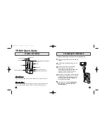
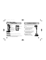
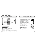
Photo: XP-ZV700

s 3ONY.(7-!!RECHARGEABLEBATTERY

6$#¾

s 3ONY.(!!"$RECHARGEABLEBATTERY

,

M!H

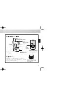
s !#POWERADAPTOR$#).6JACK

US and foreign patents licensed from Dolby Laboratories.

%XCEPT:6

: AEP

MODEL&ORTHEAREACODE

OFTHEMODELYOUPURCHASEDCHECKTHEUPPERLEFT
SIDEOFTHEBARCODEONTHEPACKAGE

120 V, 60 Hz (MX model)

220 V, 50 Hz (AR model)

230 V, 50 Hz (HK model)

240 V, 50 Hz (AUS model)

100 V-240 V, 50/60 Hz (Other models)

Summary of Contents for XP-ZV700

Page 1: ...3 and other patents issued or pending Gracenote and CDDB are registered trademarks of Gracenote The Gracenote logo and logotype the Gracenote CDDB logo and the Powered by Gracenote logo are trademarks of Gracenote Program 2001 2002 2003 2004 Sony Corporation Documentation 2004 Sony Corporation 3YSTEM OMPACT DISC DIGITAL AUDIO SYSTEM ASER DIODE PROPERTIES ATERIAL A L S 7AVELENGTH L NM MISSION DURAT...

Page 2: ...CONNECT IT FROM THE OUTLET IMMEDIATELY 2ECORDED AT KBPS 2ECORDED AT KBPS HARGING TIME VARIES DEPENDING ON HOW THE RECHARGEABLE BATTERY IS USED XCEPT 6 AEP MODEL PERATING TEMPERATURE IMENSIONS W H D EXCLUDING PROJECTING PARTS AND CONTROLS PPROX MM b b IN ASS EXCLUDING ACCESSORIES PPROX G OZ ESIGN AND SPECIlCATIONS ARE SUBJECT TO CHANGE WITHOUT NOTICE s bbreviation POWER ADAPTOR Except 6 AEP MODEL A...

Page 3: ...e objective lens will move up and down 2 times along with inward motion for the focus search NOTES ON REPLACEMENT OF EGL BOARD OR EEPROM IC1602 When EGL board is replaced or EEPROM IC1602 on the EGL board is replaced patch processing is needed Confirm about information of patch processing to each service headquarters Fig 1 Method to push the S502 UNLEADED SOLDER Boards requiring use of unleaded so...

Page 4: ... recommended Hard disk drive space 200 MB or more 1 5 GB or more is recommended The amount space will vary according to Windows version and the number of music files stored on the hard disk RAM 64 MB or more 128 MB or more is recommended Others CD drive capable of digital playback by WDM Sound Board USB port supports USB previously USB 1 1 Operating System Factory installed Windows XP Media Center...

Page 5: ...dels x CHG button Remote xbutton 3 CD player u play pause ENTER button Remote u play pause button 4 buttons 5 buttons 6 DISPLAY MENU button 7 CD player VOL f F buttons VOL f F Remote VOL 8 i headphones jack 9 DC IN 3 V jack q HOLD switch on the back of the CD player qa OPEN switch qs Clip This button has a tactile dot E18 Singapore model Abbreviation ISPLAY Ȯ HARACTER INFORMATION DISPLAY ȯ TRAC PL...

Page 6: ...numerical order given 3 2 CABINET UPPER ASSY CABINET LOWER Page 6 3 4 SWITCH BOARD Page 7 3 3 JACK BOARD OPTICAL PICK UP ASSY CDM 3325ERV Page 7 SET 1 Open the upper lid 4 cabinet lower 5 flexible flat 12 core cable CN601 6 cabinet upper assy S501 knob hold Note On installation of JACK board adjust the position of switch S501 and knob hold 3 two claws 3 two claws 3 two claws 2 two screws 2 four sc...

Page 7: ... CN601 5 optical pick up assy CDM 3325ERV 3 JACK board 4 insulator 4 insulator 4 insulator 2 two connectors CN401 CN402 1 Open the upper lid 2 eight screws 4 cover SW PWB 5 flexible flat 12 core cable CN1002 3 claw 6 liquid crystal display panel LCD1001 CN1001 7 SWITCH board 9 button operation 8 button menu ...

Page 8: ... f internal tolerance C panel designation A B Line Power voltage is dc 1 5V and fed with regulated dc power supply from battery terminal Voltages and waveforms are dc with respect to ground under no signal conditions no mark CD PLAY Voltages are taken with a VOM Input impedance 10 MΩ Voltage variations may be noted due to normal produc tion tolerances Waveforms are taken with a oscilloscope Voltag...

Page 9: ...C664 C646 C663 R613 R644 R653 R642 C659 C677 R604 C610 C603 R629 R638 R636 R637 R609 C608 C654 C653 C649 R628 R608 R639 C648 R634 C642 R635 C650 R656 R655 R650 R651 R649 C624 C626 C618 R669 C602 RB601 C601 R603 C694 CN601 C609 50 26 25 1 1 15 OPTICAL PICK UP BLOCK DAX 25EV A B C D E F G H I 1 2 3 4 5 6 7 8 9 10 JACK BOARD CN501 Page 11 A ZV700 E18 E33 MX HK AR AUS ZV701 E18 IC604 IC1602 IC603 Ver ...

Page 10: ...AOUTR AOUTL BEEP PWRSW XRST POWERLT SO0 SXCK0 COLDST XADEVENT SYNC CASINO_WAKE MUTE MDP FG SRDR SFDR TRDR TFDR FRDR FFDR LCD_SDT_I LCD_SDT_O LCD_XSCR_O LCD_CS LCD_XRST AD_KEY2 AD_KEY1 CNGMNT HOLD OPEN DCINMNT AD_RMKEY TSB FE A SE B CE E TE F T T F F F F T T SDDQ1 SDDQ2 SDDQ3 SDDQ4 SDDQ5 SDDQ6 SDDQ7 SDDQ8 SDLDQM SDXWE SDXCAS SDXRAS SDXCS SDA11 SDA10 SDA0 SDA1 SDA2 SDA3 SDDQ9 SDDQ10 SDDQ11 SDDQ12 SD...

Page 11: ...C419 Q401 D405 D404 D407 R430 R429 C422 C441 L411 L412 C438 L414 L416 L415 R457 D411 C431 C443 C428 R442 R441 R443 R440 C429 Q408 Q410 R427 C403 C432 C409 FB404 C405 FB401 R439 R502 R504 C501 C502 VDR401 FB402 C407 R305 C311 FB303 L201 R203 L501 C202 C102 C301 L301 C304 R301 C308 C305 CN501 CN402 CN401 C423 C402 R407 C302 C208 C108 13 12 1 24 SL501 OPEN JACK BOARD COMPONENT SIDE 1 864 027 11 11 1 ...

Page 12: ...17 R432 R428 R455 C439 R419 C425 R416 C435 C434 R433 R403 C436 C411 R415 R507 R423 D406 C426 R417 R413 C444 D408 C433 C412 C413 R431 Q409 R426 R425 R424 R421 C503 C437 R404 R405 C504 FB502 R402 R411 C404 TH401 D303 D304 VDR309 D301 C107 R104 D101 D201 L101 C207 R204 R103 C204 R201 R101 R102 C104 C103 R111 C203 R211 C307 C303 R202 FB605 FB604 FB603 FB602 FB601 FB608 FB607 FB606 C601 C602 CN601 F401...

Page 13: ... F T T S S RS CHGSW DATA_O DATA_I AD_KEY1 AD_KEY2 COM W V U S S SRDR SFDR CHGMNT TFDR TRDR FFDR FRDR DATA CLOCK COLDST WAKE SYNC RSTB BEEP MUTE PWRSW LCH RCH AD_RMKEY HOLD OPEN CASINO_WAKE AD_RMKEY DCINMNT OPEN HOLD CHGMNT AD_KEY1 AD_KEY2 XRST_I LCD_CS_I CLK_I DATA_O DATA_I FFDR FRDR TFDR TRDR SFDR SRDR FG MDP F F T T MUTE CASINO_WAKE SYNC WAKE COLDST CLOCK DATA LATCHB RSTB VAPC PAPC PWRSW BEEP LC...

Page 14: ...004 S1008 S1003 S1001 R1005 R1004 R1003 R1002 R1001 CN1002 R1135 R1102 R1103 R1101 R1105 R1109 R1114 R1106 S1009 C1008 CN1001 C1007 C1006 C1003 C1004 C1005 C1010 C1011 C1012 C1002 S1002 SWITCH BOARD 1 864 579 1 23 LCD1001 LIQUID CRYSTAL DISPLAY B JACK BOARD CN601 Page 12 1 12 v VOL VOL V u ENTER DISPLAY MENU B SEARCH b x CHG x ZV700 AEP EXCEPT ZV700 AEP A B C D E F G 1 2 3 4 5 6 7 8 11 11 ...

Page 15: ...009 S1008 S1007 R1135 C1012 C1003 C1011 C1004 C1010 C1005 C1006 C1008 0 22 1k 1k 1k 1k 1k 10k 4 7k 2 2k 22k 2 2k 10k 22k 2 2k 2 2k 22k 12P 23P 1k 47k 4 7k 4 7k 0 1 0 1 0 0 22 0 22 0 22 0 22 0 22 0 22 0 22 0 47 SCK CSB SDI SDO RSTB VDD VSS VREF VCIN CP1 CN1 CP2 CN2 CP3 CN3 VSSL VCOUT VLCIN V1 V2 V3 V4 V5 CLK_I LCD_CS_I DATA_O DATA_I LCD_XRST D_GND AD_KEY1 AD_KEY2 PS SGND SEARCH ENTER VOL VOL DISPLA...

Page 16: ...14 TAPTDO Not used 15 16 SDDQ14 SDDQ13 I O Two way data bus with the SD RAM 17 SCANEN Not used 18 19 SDDQ12 SDDQ11 I O Two way data bus with the SD RAM 20 TEST2 Not used 21 22 SDDQ10 SDDQ8 I O Two way data bus with the SD RAM 23 VDIOSD0 Power supply terminal 2 7V 24 VSS1 Ground terminal 25 to 28 SDDQ9 SDDQ6 SDDQ7 SDDQ2 I O Two way data bus with the SD RAM 29 TEST3 Not used 30 31 SDDQ4 SDDQ3 I O Tw...

Page 17: ... used 82 PI0 PCMDO Not used 83 ADCLK Not used 84 DOUT Not used 85 PJ7 MON7 MONCK Not used 86 PJ6 MON6 MONDO Not used 87 PJ5 MON5 O Amplifier power on off control signal output to the headphone amplifier H amplifier power on 88 to 91 PJ4 MON4 to PJ1 MON1 Not used 92 XRST_PWR_O Not used 93 VSS6 Ground terminal 94 VDIO2 Power supply terminal 2 1V 95 DVDD1 Power supply terminal 1 3V 96 AVDDA1 Power su...

Page 18: ...Ground terminal 137 AVDSAD Power supply terminal 2 1V 138 IGEN I Stabilized current input for operational amplifiers 139 FE A I A signal input from the optical pick up block 140 SE B I B signal input from the optical pick up block 141 TE F I F signal input from the optical pick up block 142 CE E I E signal input from the optical pick up block 143 VC I Middle point voltage input terminal Not used 1...

Page 19: ... data output to the power control and EEPROM 178 PC0 SCK0 O Serial clock signal output to the power control and EEPROM 179 VSS15 Ground terminal 180 VDIO5 Power supply terminal 2V 181 PG7 I Cold start flag input from the power control 182 183 PG6 PG5 Not used 184 PG4 O Reset signal output to the liquid crystal display 185 186 PG3 PG2 Not used 187 PG1 O Standby signal output to the optical pick up ...

Page 20: ...C0 Not used 217 PE7 XSCS1 O Command latch signal output to the liquid crystal display 218 NCS1 Not used 219 to 237 A0 A19 to A1 Not used 238 NRD Not used 239 NWE Not used 240 to 255 DQ15 to DQ0 Not used 256 VDD_FL1 Power supply terminal Not used 257 VSS_FL1 Ground terminal 258 VDD_SR1 Power supply terminal Not used 259 VSS_SR1 Ground terminal 260 VDD_SR2 Power supply terminal Not used 261 VSS_SR2 ...

Page 21: ...NC I 176 4 kHz clock signal input from the system controller 24 WAKE I Wake up signal input from the system controller 25 COLDST O Cold start flag output to the system controller 26 CLOCK I Serial clock signal input from the system controller 27 DATA I Serial data input from the system controller 28 LATCHB I Command latch signal input from the system controller 29 EXTRSTB I External reset signal i...

Page 22: ...ching power supply circuit 59 INPVD I Error amplifier non invert input of VD switching power supply circuit 60 INP0 I Error amplifier non invert input of VCC0 switching power supply circuit 61 RF Error amplifier connection terminal of APC circuit 62 INM O Error amplifier output terminal of APC circuit 63 PAPC I Feed back voltage input terminal of APC circuit 64 VAPC O Voltage output terminal of AP...

Page 23: ...n Ref No Part No Description Remark Ref No Part No Description Remark 1 2 342 680 01 SPRING FULL OPEN L 2 2 342 679 01 SPRING FULL OPEN R 3 3 254 058 11 SCREW 4 2 188 316 21 LID BATTERY CASE WHITE 4 2 188 316 31 LID BATTERY CASE BLACK 5 2 187 912 21 KNOB OPEN WHITE 5 2 187 912 31 KNOB OPEN BLACK 6 2 187 914 01 SPRING OPEN 7 2 187 913 01 LEVER OPEN 8 3 034 792 11 SCREW TAPPING B2 0 9 3 261 240 02 L...

Page 24: ...ET UPPER SUB ASSY B BLACK ZV702 51 X 2050 977 1 CABINET UPPER SUB ASSY W WHITE ZV700 AEP 5 2 CABINET UPPER ASSY SECTION 51 X 2050 978 1 CABINET UPPER SUB ASSY B BLACK ZV700 AEP 52 2 189 517 01 BUTTON OPERATION GROUP VOL GROUP u ENTER x VOL SEARCH 53 2 342 711 01 SHEET MENU INSULATING 54 A 1083 828 A SWITCH BOARD COMPLETE 55 1 829 981 11 CABLE FLEXIBLE FLAT 12 CORE 56 2 189 518 01 COVER SW PWB WHIT...

Page 25: ...V700 AEP 104 2 187 917 01 SPRING COIL EXCEPT ZV700 AEP 104 2 187 917 11 SPRING COIL ZV700 AEP 105 A 1098 954 A EGL BOARD COMPLETE ZV700 AEP ZV701 AEP ZV702 105 A 1098 956 A EGL BOARD COMPLETE ZV700 E18 E33 MX HK AR AUS ZV701 E18 106 2 589 207 01 SHIELD CUSHION 107 2 187 915 51 CABINET LOWER WHITE 107 2 187 915 61 CABINET LOWER BLACK 108 2 188 315 21 KNOB HOLD WHITE 108 2 188 315 31 KNOB HOLD BLACK...

Page 26: ...SPRING SLED 156 A 1061 631 A SCREW FEED ASSY 157 3 221 268 01 GEAR B 158 3 221 475 01 SHAFT STANDARD 159 3 222 298 01 RACK 160 3 222 299 01 SPRING RACK RETAINER 161 3 348 998 31 SCREW M1 4X2 5 TAPPING PAN M401 A 1061 632 A TABLE ASSY TURN SPINDLE M402 A 1061 630 A MOTOR ASSY SLED Ref No Part No Description Remark Ref No Part No Description Remark The components identified by mark 0 or dotted line ...

Page 27: ... L RESISTOR FERRITE BEAD R406 1 218 990 11 SHORT CHIP 0 R407 1 218 990 11 SHORT CHIP 0 R602 1 218 990 11 SHORT CHIP 0 R603 1 218 929 11 RES CHIP 10 5 1 16W R604 1 218 929 11 RES CHIP 10 5 1 16W R606 1 218 990 11 SHORT CHIP 0 R608 1 218 973 11 RES CHIP 47K 5 1 16W R609 1 218 969 11 RES CHIP 22K 5 1 16W R610 1 218 977 11 RES CHIP 100K 5 1 16W R613 1 218 990 11 SHORT CHIP 0 R614 1 218 990 11 SHORT CH...

Page 28: ... 6 3V C409 1 137 710 11 CERAMIC CHIP 10uF 20 6 3V C410 1 128 003 11 ELECT CHIP 22uF 20 4V C411 1 162 970 11 CERAMIC CHIP 0 01uF 10 25V C412 1 162 970 11 CERAMIC CHIP 0 01uF 10 25V C413 1 162 970 11 CERAMIC CHIP 0 01uF 10 25V C414 1 117 863 11 CERAMIC CHIP 0 47uF 10 6 3V C416 1 162 927 11 CERAMIC CHIP 100PF 5 50V C417 1 117 863 11 CERAMIC CHIP 0 47uF 10 6 3V C418 1 126 208 21 ELECT CHIP 47uF 20 4V ...

Page 29: ... 602 21 TRANSISTOR 2SC4154 F RESISTOR R101 1 216 841 11 METAL CHIP 47K 5 1 10W R102 1 216 837 11 METAL CHIP 22K 5 1 10W R103 1 216 817 11 METAL CHIP 470 5 1 10W R104 1 218 446 11 METAL CHIP 1 5 1 10W R111 1 216 825 11 METAL CHIP 2 2K 5 1 10W R201 1 216 841 11 METAL CHIP 47K 5 1 10W R202 1 216 837 11 METAL CHIP 22K 5 1 10W R203 1 216 817 11 METAL CHIP 470 5 1 10W R204 1 218 446 11 METAL CHIP 1 5 1 ...

Page 30: ...METAL CHIP 22K 5 1 10W R1105 1 216 825 11 METAL CHIP 2 2K 5 1 10W R1106 1 216 829 11 METAL CHIP 4 7K 5 1 10W R1107 1 216 833 11 METAL CHIP 10K 5 1 10W R1108 1 216 837 11 METAL CHIP 22K 5 1 10W R1109 1 216 821 11 METAL CHIP 1K 5 1 10W R1110 1 216 825 11 METAL CHIP 2 2K 5 1 10W R1111 1 216 825 11 METAL CHIP 2 2K 5 1 10W R1112 1 216 837 11 METAL CHIP 22K 5 1 10W R1113 1 216 841 11 METAL CHIP 47K 5 1 ...

Page 31: ...70 for WHITE ZV700 E18 HK AUS 502 1 542 529 21 HEADPHONE HP M170 for WHITE ZV701 E18 503 8 912 734 90 EARPHONES HP SC021SP WC SET for WHITE ZV702 503 8 912 737 90 EARPHONES HP SC021LP WC SET for WHITE ZV700 AEP E33 MX AR ZV701 AEP 503 8 912 739 90 HEADPHONE HP SC021SP BC SET for BLACK ZV702 503 8 912 740 90 HEADPHONE HP SC021LP BC SET for BLACK ZV700 AEP E33 AR ZV701 AEP 504 1 478 544 11 REMOTE CO...

Page 32: ...n and New Zealand models to XP ZV700 Revision of electrical parts 1 2 2005 04 Addition of Mexican model to XP ZV700 1 3 2005 07 Deletion of Part No for Ref No IC603 on EGL board and Deletion of Notes on replacement of Ref No IC603 Change of Part No for JACK board SPM 05091 05105 1 4 2005 10 Addition of NOTES ON REPLACEMENT OF EGL BOARD OR EEPROM IC1602 Change of Part No for EGL board Change of Par...

Reviews: