background image

UM021204-0508

 Schematics

Z8 Encore! XP

®

 Dual F1680 Series Development Kit

User Manual

12

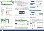
Figure 6. Z8 Encore! XP Dual F1680 Series MCU Development Board (Continued)

5

5

4

4

3

3

2

2

1

1

D

D

C

C

B

B

A

A

ANA7

PCM_1

ANA3

PC3_SCK

PC4_MOSI

GND

ANA5

SDA

GND

VCC_3.3V

ANA4

GND

PC2_nSS

GND

ANA0

SCL

nCTS1

RXD0

PCM_0

ANA1

PC5_MISO

nCTS0

ANA2

RXD1

-RESET

VCC_3.3V

GND

ANA6

TXD0

GND

ANA1
ANA0

ANA2

ANA2

ANA3

ANA7

ANA6

ANA5

ANA4

ANA1

ANA0

PC6_T2IN
PC7_T2OUT

ANA4

ANA7

PCM_0
PCM_1
PCM_2

PC2_nSS

PCM_3

PC3_SCK

PCM_4

PC4_MOSI

PCM_5

PC5_MISO

PCM_6

PC6_T2IN

PCM_7

PC7_T2OUT

PES_0

SCL

PES_1

SDA

PES_2
PES_3

GND

GND

GND

PBM_5

GND

PES_5

GND

PEM_6

PDM_1
PDM_2
PDM_3

PAS_3

PAS_5
PAS_6
PAS_7

PBM_3
PBM_4

PEM_3
PEM_4
PEM_5

PAS_4

PDS_1

PES_6

PCS_4

PCS_3

PDS_2

PBM_2

PBM_1

PBM_0

PAS_2

-DIS_232
-DIS_IrDA

ANA[7:0]

RXD1

nCTS1

-RESET

PAS_[7:2]

PES_[3:0]

PAM_0

PAM_1

PAM_6

PDM_6

PEM_0

PBM_[5:0]

PCM_[7:0]

PDM_[3:1]

PEM_[6:3]

TXD1

TXD0

nCTS0
RXD0

PDS_[2:1]

PDS_7

PBS_5

PCS_[4:3]

PDM_7

PES_[6:5]

PES_4

VCC_3.3V

VCC_3.3V

Title

Size

Document Number

Rev

Date:

Sheet

of

96C1011-001

C

Z8F248xB Evaluation Module. Schematic.

B

3

4

Wednesday, November 29, 2006

Title

Size

Document Number

Rev

Date:

Sheet

of

96C1011-001

C

Z8F248xB Evaluation Module. Schematic.

B

3

4

Wednesday, November 29, 2006

Title

Size

Document Number

Rev

Date:

Sheet

of

96C1011-001

C

Z8F248xB Evaluation Module. Schematic.

B

3

4

Wednesday, November 29, 2006

NC

NC

NC

NC

NC

NC

NC

NC

NC

NC

If Module is plugged onto the Dev Platform the local 
RS232 interface is disabled by pin 50 of JP2

MDS INTERFACE

NC
NC

C8

0.1uF

C8

0.1uF

1

2

C4

0.1uF

C4

0.1uF

1

2

C7

0.1uF

C7

0.1uF

1

2

JP2

HDR/PIN 30x2

JP2

HDR/PIN 30x2

1

1

2

2

3

3

4

4

5

5

6

6

7

7

8

8

9

9

10

10

11

11

12

12

13

13

14

14

15

15

16

16

17

17

18

18

19

19

20

20

21

21

22

22

23

23

24

24

25

25

26

26

27

27

28

28

29

29

30

30

31

31

32

32

33

33

34

34

35

35

36

36

37

37

38

38

39

39

40

40

41

41

42

42

43

43

44

44

45

45

46

46

47

47

48

48

49

49

50

50

51

51

52

52

53

53

54

54

55

55

56

56

57

57

58

58

59

59

60

60

C10

0.1uF

C10

0.1uF

1

2

C3

0.1uF

C3

0.1uF

1

2

C6

0.1uF

C6

0.1uF

1

2

C9

0.1uF

C9

0.1uF

1

2

C5

0.1uF

C5

0.1uF

1

2

JP1

HDR/PIN 30x2

JP1

HDR/PIN 30x2

1

1

2

2

3

3

4

4

5

5

6

6

7

7

8

8

9

9

10

10

11

11

12

12

13

13

14

14

15

15

16

16

17

17

18

18

19

19

20

20

21

21

22

22

23

23

24

24

25

25

26

26

27

27

28

28

29

29

30

30

31

31

32

32

33

33

34

34

35

35

36

36

37

37

38

38

39

39

40

40

41

41

42

42

43

43

44

44

45

45

46

46

47

47

48

48

49

49

50

50

51

51

52

52

53

53

54

54

55

55

56

56

57

57

58

58

59

59

60

60

Summary of Contents for Z8 Encore! XP Dual F1680 Series

Page 1: ...Copyright 2008 by Zilog Inc All rights reserved www zilog com Z8F16800144ZCOG Z8 Encore XP Dual F1680 Series Development Kit User Manual UM021204 0508 ...

Page 2: ...nge to this document from its previous revision For more details refer to the corresponding pages and appropriate links in the table below Date Revision Level Description Page No May 2008 04 Updated Introduction section 1 February 2008 03 Updated Zilog logo and changed ZiLOG to Zilog All June 2007 02 Removed IrDA 2 6 8 10 November 2006 01 Original issue All ...

Page 3: ...on 1 MCU Features 1 Hardware Supported Software Features 3 Z8 Encore XP Dual F1680 Series Development Board 4 Theory of Operation 5 Block Diagram 7 Hardware Interface Specification 8 Power and Communication Interfaces 8 External Interface Headers JP1 and JP2 9 Kit Contents 9 Installation 9 Schematics 10 Customer Support 14 ...

Page 4: ...applications include Wide operating voltage range 1 8 V 3 6 V Active Halt and Stop operational modes with the ability to enable or disable peripherals for power savings Oscillator control that determines clock source operating speed and fail safe operation in addition to fast wakeup A user controlled Program RAM area to store interrupt service routines ISR of high frequency interrupts The Program ...

Page 5: ...ee enhanced 16 bit timers with Capture Compare and PWM capability Multichannel timer that supports four capture compare modules on one timer Watchdog Timer WDT with dedicated internal RC oscillator 39 Input Output I O pins Up to 20 vectored interrupts On Chip Debugger OCD Power On Reset POR Built in Low Voltage Detection LVD and Voltage Brownout VBO protection Internal Precision Oscillator IPO wit...

Page 6: ...tor improving execution time and decreasing the required Program Memory Software stack allows greater depth in sub routine calls and interrupts more than hardware stacks Compatible with existing Z8 code Expanded internal Register File allows access up to 4 KB New instructions improve execution efficiency for code developed using higher level programming languages including C Pipelined instruction ...

Page 7: ...8 Encore XP Dual F1680 Series Development Board The Z8 Encore XP Dual F1680 Series development board see Figure 1 provides a tool to evaluate features of the Z8 Encore XP F1680 Series MCU and to start developing an application before building the hardware Figure 1 Z8 Encore XP F1680 Series Development Board ...

Page 8: ...ned below The features of Z8F1680 MDS compliant module include Two Z8F1680 devices the Z8F1680_M I2 C Master device and the Z8F1680_S I2 C Slave device Terms Definitions Z8F1680_S MCU_S I2 C Slave device Z8F1680_M MCU_M I2 C Master device HyperTerminal Console Serial Port XModem UART0 UART1 DBG1 DBG2 MCU_S U1 MCU_M U3 MCU_M MCU_S S2 DBG USB Smart Cable ZDS II Debugger PC0 PC1 PC2 RED_LED YELLOW_LE...

Page 9: ... source for the Slave device and needs to be configured as an output with Open Drain Downloading and debugging code in either the Master or Slave device using the standard OCD interface on either chip The operation mode is selected by switch S2 All the GPIOs of both devices except for those used on the module are connected to JP1 and JP2 All the GPIOs of the Slave device except analog inputs are c...

Page 10: ...ual F1680 Series Development Kit User Manual UM021204 0508 Z8 Encore XP Dual F1680 Series 7 Block Diagram Figure 3 displays the block diagram of the Z8F1680 MDS module Figure 3 Block Diagram of the Z8F1680 MDS Module ...

Page 11: ...erning the shunt status functions devices and defaults affected of jumpers JP1 JP2 JP3 JP4 JP5 and JP6 Table 1 Shunt Settings for the Z8 Encore XP F1680 Development Board Number Shunts Function Pins Connected IN OUT Factory Settings 1 J1 AN3_IN 1 2 AN3_IN connected to AN3 on the JP3 2 3 2 3 AN3_IN connected to Vout of DAC Default 2 J2 RS 232 IN RS 232 disabled Default OUT RS 232 enabled OUT 4 J4 A...

Page 12: ...and JP2 are displayed in the schematic in Figure 5 on page 11 Kit Contents For kit contents refer to Z8 Encore XP Dual F1680 Series Develop ment Kit Quick Start Guide QS0038 Installation Follow the directions in the Z8 Encore XP Dual F1680 Series Develop ment Kit Quick Start Guide QS0038 for software installation and setup of the Z8 Encore XP Dual F1680 Series Development Kit ...

Page 13: ... C Z8F24xB Evaluation Module Schematic B 1 4 Wednesday November 29 2006 Title Size Document Number Rev Date Sheet of 96C1011 001 C Z8F24xB Evaluation Module Schematic B 1 4 Wednesday November 29 2006 Title Size Document Number Rev Date Sheet of 96C1011 001 C Z8F24xB Evaluation Module Schematic B 1 4 Wednesday November 29 2006 TOP POWER COMMUNICATIONS POWER COMMUNICATIONS PA4_RXD0 PCS_6 PCS_5 DIS_I...

Page 14: ... 6 2C 3 GND 4 VCC 8 U7A SN74LVC2G66 U7A SN74LVC2G66 2A 1 2B 2 2C 7 GND 4 VCC 8 C29 0 1uF C29 0 1uF C2 22pF C2 22pF C21 0 1uF C21 0 1uF C31 0 1uF C31 0 1uF R3 10K R3 10K 1 2 C32 10uF C32 10uF 1 2 U2 DAC7571 U2 DAC7571 Vout 1 GND 2 VCC 3 SDA 4 SCL 5 A0 6 C30 0 1uF C30 0 1uF R2 3 3K R2 3 3K 1 2 C22 0 1uF C22 0 1uF R4 10K R4 10K 1 2 U12 SN74LVC1G125 U12 SN74LVC1G125 OE 1 A 2 GND 3 Y 4 VCC 5 J8 SHUNT J...

Page 15: ... Number Rev Date Sheet of 96C1011 001 C Z8F248xB Evaluation Module Schematic B 3 4 Wednesday November 29 2006 Title Size Document Number Rev Date Sheet of 96C1011 001 C Z8F248xB Evaluation Module Schematic B 3 4 Wednesday November 29 2006 NC NC NC NC NC NC NC NC NC NC If Module is plugged onto the Dev Platform the local RS232 interface is disabled by pin 50 of JP2 MDS INTERFACE NC NC C8 0 1uF C8 0...

Page 16: ...R2 1 2 C13 0 1uF C13 0 1uF 1 2 C19 0 1uF C19 0 1uF 1 2 U10B SN74LVC2G04 U10B SN74LVC2G04 I 3 4 O 2 GND 5 VCC P1 CON DC P1 CON DC 2 3 1 S1 SW PB NO S1 SW PB NO A B B1 A1 D2 GREEN D2 GREEN 2 1 P2 DB9 Female P2 DB9 Female 5 9 4 8 3 7 2 6 1 C16 0 1uF C16 0 1uF 1 2 D4 YELL D4 YELL 2 1 R15 10K R15 10K 1 2 C12 0 1uF C12 0 1uF 1 2 R12 10K R12 10K 1 2 C20 0 33uF C20 0 33uF J9 SHUNT J9 SHUNT R13 68R R13 68R...

Page 17: ...port For answers to technical questions about the product documentation or any other issues with Zilog s offerings please visit Zilog s Knowledge Base at http www zilog com kb For any comments detail technical questions or reporting problems please visit Zilog s Technical Support at http support zilog com ...

Page 18: ...o perform can be reasonably expected to cause the failure of the life support device or system or to affect its safety or effectiveness Document Disclaimer 2008 by Zilog Inc All rights reserved Information in this publication concerning the devices applications or technology described is intended to suggest possible uses and may be superseded ZILOG INC DOES NOT ASSUME LIABILITY FOR OR PROVIDE A RE...

Reviews: