5 Encoder Interfaces
5.1.1 Overview
5-2
5.1
A quad B Pulse interface
5.1.1
Overview
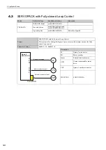
A quad B pulse signals is counted by each edges in the master. The interface block diagram is shown below.
5.1.2
Technical Data
.
5.1.3
Connection
*1 Without hall sensor, do not connect to any signals. With hall sensor, please refer to section 6-1, too.
*2 Pins denoted as N.C. do not connect to any signals.
A quad B
Pulse
encoder
Encoder Master
A
B
FPGA
REF
Servo
Serial
I/F
Items
Description
Encoder Supply
Output voltage
Typically 5 V
Incremental Encoder
Input
Signal form
Square wave pulse
Evaluation
4x
Max. input frequency
1 MHz
Max. counter frequency
4 MHz
Max. reference frequency 1 MHz
Distance between edges
0.2 µsec or more
Differential voltage
0.2 V or more
No
Signal
Pin Function
Dir.
No
Signal
Pin Function
Dir.
1
N.C. *2
OUT
14
-
N.C. *2
I/O
2
N.C. *2
OUT
15
-
N.C. *2
I/O
3
V
Hall Signal V + *1
IN
16
W
Hall Signal W + *1
IN
4
U
Hall Signal U + *1
IN
17
PG_0V
Ground
-
5
/C(Z)
Pulse /C(Z)
-
18
-
N.C. *2
-
6
C(Z)
Pulse C(Z)
-
19
-
N.C. *2
-
7
-
N.C. *2
-
20
-
N.C. *2
-
8
PG+5V
Power
OUT
21
-
N.C. *2
-
9
PG+5V
Power
OUT
22
-
N.C. *2
-
10
PG+5V
Power
OUT
23
A
Pulse A
-
11
PG_0V
Ground
-
24
/A
Pulse /A
-
12
PG_0V
Ground
-
25
B
Pulse B
-
13
PG_0V
Ground
-
26
/B
Pulse /B
-
Summary of Contents for S-V Seres
Page 16: ...xvi ...
Page 62: ...9 Motor and Scale Parameter File 9 2 2 Scale Parameters 9 6 ...


