background image

17

R-S300

R-S30

0

Fig. 5

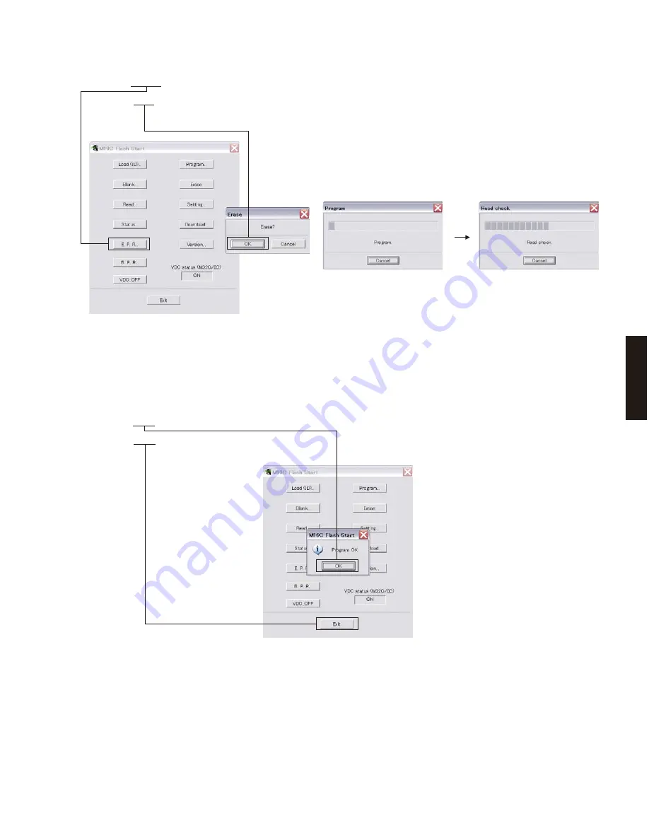
6.  Click [E.P.R.], then the “Erase” screen appears. (Fig. 5)

7.  Click [OK] to start writing. (Fig. 5)

Writing being executed.

10. Disconnect the power cable of this unit from the AC outlet.

11. Remove the RS-232C conversion adaptor and flexible flat cable from the writing port of this unit.

12. Connect the power cable of this unit to the AC outlet, start up the self-diagnostic function and check that the 

firmware version and checksum are the same as written ones. (See “Confirmation of firmware version and 
checksum”)

Fig. 6

8.  When writing of the firmware is completed, the screen appears as shown below. (Fig. 6)

Click [OK]. (Fig. 6)

9.  Click [Exit] to end FlashSta.exe. (Fig. 6)

Summary of Contents for R S300

Page 1: ...te and applicable to the unit s indicated on the cover The research engineering and service departments of YAMAHA are continually striving to improve YAMAHA products Modifications are therefore inevitable and specifications are subject to change without notice or obligation to retrofit Should any discrepancy appear to exist please contact the distributor s Service Division WARNING Static discharge...

Page 2: ... DE MÉME TYPE DE 5A 125V All of the P C B s installed in this unit and solder joints are soldered using the lead free solder Among some types of lead free solder currently available it is recommended to use one of the following types for the repair work Sn Ag Cu tin silver copper Sn Cu tin copper Sn Zn Bi tin zinc bismuth Caution As the melting point temperature of the lead free solder is about 30...

Page 3: ...3 R S300 R S300 IMPEDANCE SELECTOR WARNING Do not change the setting of the IMPEDANCE SELECTOR switch when the unit power is switched on as doing so may damage the unit IMPEDANCE SELECTOR ...

Page 4: ...4 R S300 R S300 R S300 U C R A L models R S300 G model FRONT PANELS ...

Page 5: ...5 R S300 R S300 R S300 A model REAR PANELS R S300 R model R S300 U C models ...

Page 6: ...6 R S300 R S300 R S300 L model R S300 G model ...

Page 7: ...7 R S300 R S300 REMOTE CONTROL PANEL RAX23 ...

Page 8: ...tion 20 Hz to 20 kHz 8 ohms 0 04 THD 50 W 50 W Dynamic Power Per Channel IHF 8 6 4 2 ohms 70 77 89 100 W MAX Power Per Channel 1 kHz 0 7 THD 4 ohms G model 55 W IEC Power 1 kHz 0 04 THD 8 ohms G model 52 W Power Band Width 0 06 THD 25 W 8 ohms 10 Hz to 50 kHz Damping Factor SPEAKER A 1 kHz 8 ohms 150 or more Maximum Effective Output Power 1 kHz 10 THD JEITA R L models 8 ohms 85 W Input Sensitivity...

Page 9: ...ple Inc registered in the U S and other countries Bluetooth is a registered trademark of the Bluetooth SIG and is used by Yamaha in accordance with a license agreement Front view Top view 435 17 1 8 335 13 1 4 50 2 151 5 7 8 130 5 1 8 21 7 8 20 5 3 4 25 5 1 387 15 1 4 341 13 3 8 55 2 1 8 46 1 3 4 240 9 1 2 ø 60 ...

Page 10: ...14 15 16 17 18 19 20 21 22 INTERNAL VIEW SERVICE PRECAUTIONS Safety measures Some internal parts in this product contain high voltages and are dangerous Be sure to take safety measures during servicing such as wearing insulating gloves Note that the capacitors indicated below are dangerous even after the power is turned off because an electric charge remains and a high voltage continues to exist t...

Page 11: ...s in the order as numbered Disconnect the power cable from the AC outlet 1 Removal of Top Cover a Remove 4 screws 4 screws and screw Fig 1 b Remove the top cover Fig 1 2 Removal of Front Panel Unit a Remove screw and then remove the support top Fig 1 b Pull out the knobs and caps Fig 1 c Remove 7 screws Fig 1 d Remove the front panel unit Fig 1 ...

Page 12: ...ove 2 screws and screw Fig 2 b Remove CB11 CB101 CB503 505 CB513 CB706 CB801 and CB805 Fig 2 c Release 2 hooks and then remove the sub chassis unit Fig 2 4 Removal of AM FM Tuner a Remove 2 screws Fig 3 b Remove CB403 Fig 2 c Remove the AM FM tuner Fig 2 5 Removal of FUNCTION 1 3 and DOCK P C B s a Remove 7 screws Fig 3 b Remove screw and screw Fig 2 c Remove CB2 CB14 CB21 and CB506 Fig 2 d Remove...

Page 13: ...e cloth and check it Fig 4 Connect the ground point of the sub chassis unit to the chassis with a ground lead or the like Fig 4 Reconnect all cables connectors that have been disconnected When connecting the flexible flat cable be careful with polarity When checking the MAIN 1 P C B Spread the rubber sheet and the cloth Then place this unit on the cloth upside down Fig 5 Remove 6 screws and then r...

Page 14: ...ve proper memorization of the set up information Start up the self diagnostic function and select 3 FACTORY PRESET menu See SELF DIAGNOSTIC FUNCTION Select 3 PRESET RSRV press the Power key to turn off the power once and turn on the power again Then the back up IC is initialized RS 232C conversion adaptor Part No WR492800 UPDATING FIRMWARE Pin No 2 RxD Pin No 2 RxD Pin No 3 TxD Pin No 3 TxD Pin No...

Page 15: ...with RS 232C cross cable RS 232C conversion adaptor and flexible flat cable as shown below Fig 1 Fig 1 Operation procedure 1 Connect the power cable of this unit to the AC outlet The power to this unit is supplied and the microprocessor is in the writing mode 2 Start up FlashSta exe The screen appears as shown below Fig 2 3 Select the data to be transmitted and port Fig 2 Select Program Select Int...

Page 16: ...is clicked the Open screen appears 4 Click Refer and select the firmware name Fig 3 The ID and MCU Type are loaded automatically when the file is selected Fig 3 Click OK Fig 3 5 Click Setting and set the baud rate Fig 4 Fig 4 115200 40 ...

Page 17: ...ptor and flexible flat cable from the writing port of this unit 12 Connect the power cable of this unit to the AC outlet start up the self diagnostic function and check that the firmware version and checksum are the same as written ones See Confirmation of firmware version and checksum Fig 6 8 When writing of the firmware is completed the screen appears as shown below Fig 6 Click OK Fig 6 9 Click ...

Page 18: ...LOOP BACK CHECK 2 BT VERSION 6 PROTECTION HISTORY 1 HISTORY 1 2 HISTORY 2 3 HISTORY 3 4 HISTORY 4 7 SIRIUS Not for service 1 SIRIUS 2 SR 3 SSP 4 MAC 5 ADP 6 PRDID 7 SEQID 8 POWER OFF FACTOR HISTORY 1 LAST 2 HISTORY 1 3 HISTORY 2 4 HISTORY 3 5 HISTORY 4 This unit has self diagnostic functions that are intended for inspection measurement and location of faulty point There are 8 main menu items each ...

Page 19: ...diagnostic function mode is activated with the protection functions disabled In this mode the SLEEP segment of the FL display flashes to indicate that the mode is self diagnostic function mode with the protection functions disabled Starting Self Diagnostic Function While pressing the DIMMER U C R A L models TP G model and PRESET keys press the Power key to turn on the power The self diagnostic fun...

Page 20: ...ction due to excess current works 1 time the power will not turn on even when the Power key is pressed In order to turn on the power again disconnect the power cable of this unit from the AC outlet once and then reconnect it again The output transistors in each amplifier channel should be checked for damage before applying power to this unit Amplifier current should be monitored by measuring DC vo...

Page 21: ...he protection function is working Cause The voltage in the power supply section is abnormal Supplementary information The protection function worked due to a defect or overload in the power supply Turning on the power without correcting the abnormality will cause the protection function to work in 1 seconds and the power supply will be shut off 2 3 When the protection function worked due to abnorm...

Page 22: ...ction menu items functions as listed below are available Power ON OFF Master volume Tone control PURE DIRECT ON OFF Functions related to the tuner and the set menu are not available Initial settings when Self Diagnostic Function started The following initial settings are used when starting self diagnostic function When self diagnostic function is canceled these settings are restored to those befor...

Page 23: ...ersion of the microprocessor IC502 on FUNCTION P C B is displayed 1 2 FIRMWARE CHECKSUM The checksum value of the microprocessor IC502 on FUNCTION P C B is displayed 1 3 SIRIUS VERSION Not for service 1 4 MODEL DESTINATION The model name and destination are displayed Destination Model 1 5 VERIFY Not for service V e r E 0 6 S u m D 8 0 2 S R V E R A 0 0 1 R 3 0 5 4 U 0 1 8 V e r i f y 2 5 5 Destina...

Page 24: ... once Segment conditions of the FL driver and the FL tube are checked by turning ON and OFF all segments Next the operation of the FL driver is checked by using the dimmer control Then a short between segments next to each other is checked by turning ON and OFF all segments alternately in lattice In the above example the segments in the second row from the top are shorted Lighting on segments in l...

Page 25: ...PRD of the IC502 is displayed Normal value 48 to 128 Reference voltage 5 0 V 255 If DC becomes out of the normal value range the protection function works to turn off the power P S 0 5 7 D C 0 9 0 3 P R E S E T I N H I 3 P R E S E T R S R V 3 FACTORY PRESET This menu is used to reserve inhibit initialization of the back up IC EEPROM IC503 on FUNCTION P C B 3 1 PRESET INHIBIT Initialization inhibit...

Page 26: ...n value of the panel key becomes out of the specified range normal operation will not be available In that case check the constant of voltage dividing resistor solder condition etc Refer to table When 4 3 KEY 0 KEY 1 sub menu is selected keys become non operable due to detection of the values of all keys However it is possible to advance to the next sub menu by turning the INPUT knob of this unit ...

Page 27: ...od No connected YDS 11 12 B YDS 12 A A D conversion value 5 0 V 255 0 32 82 109 110 146 147 175 238 255 4 5 MODEL DESTINATION MODEL Model name is detected The voltage at 72 pin MODEL of the IC502 is displayed Reference voltage 5 0 V 255 DESTINATION Destination is detected The voltage at 71 pin DEST of the IC502 is displayed Reference voltage 5 0 V 255 DOCK TYPE M D L 0 5 4 D S 0 5 4 A D conversion...

Page 28: ... BT VERSION The DOCK Bluetooth module YBA 10 version is displayed Note Be sure to return the shorted pins to their original condition after executing this test DOCK CONNECTOR 1 2 19 3 4 5 6 7 8 9 10 11 12 13 14 15 16 17 18 20 21 10 k ohms 1 4 W Check item Result Display UART loop back test OK Y NG N IPD_N_APDET iPod accessory power detection IC502 pin No 23 Low YES Y High NO N IPD_N_DET iPod insta...

Page 29: ... service 8 POWER OFF FACTOR HISTORY This menu is used to display the history of power off factor S I R I U S 8 1 P A N E L S W S R F F 0 0 F F 8 2 R E M O C O N S S P 0 0 0 0 0 0 8 3 A P D T I M E R P R D I D 0 0 0 0 0 0 M A C 0 0 0 0 0 0 8 4 P R O T E C T I O N S E Q I D 0 0 0 0 0 0 A D P 0 0 0 0 0 0 8 5 A C O F F 7 1 SIRIUS 8 1 History 1 7 2 SR 8 2 History 2 7 3 SSP 8 3 History 3 7 6 PRDID 7 4 M...

Page 30: ...he voltage across the terminals of R154 L ch and R155 R ch are between 0 1 mV and 10 mV 2 If measured voltage exceeds 10 mV open cut off R139 L ch R140 R ch and reconfirm the voltage Attention If the measured voltage exceeds 10 mV after repairing the power amplifier check other parts again for any possible defect before cutting the resistor 3 Confirm that the voltage is between 0 2 mV and 15 mV af...

Page 31: ...31 R S300 R S300 L ch R ch 0 1 mV 10 mV R139 R140 R154 R155 Cut off Cut off MAIN 1 0 1 mV 10 mV SCHEMATIC DIAGRAM ...

Page 32: ... 25 P32 24 P33 23 P34 22 P35 21 NX 20 19 15G 16G 18 14G 17 13G 16 12G 15 11G 14 10G 13 9G 12 8G 11 7G 10 6G 9 5G 8 4G 7 3G 6 2G 5 1G 4 NP 3 NP 2 NX 1 F1 27 P30 26 P31 Connection PIN CONNECTION GRID ASSIGNMENT 1 1 2 1 3 1 4 1 5 1 1 2 1 3 1 4 1 5 1 6 1 7 2 2 2 3 2 4 2 5 2 6 2 7 3 2 3 3 3 4 3 5 3 6 3 7 4 2 4 3 4 4 4 5 4 6 4 7 5 2 5 3 5 4 5 5 5 6 5 7 1G 14G 15G PATTERN AREA S2 S4 S3 S2 S5 S3 1 60 V701...

Page 33: ...2 3 2 4 2 5 2 1 3 2 3 3 3 4 3 5 3 1 4 2 4 3 4 4 4 5 4 1 5 2 5 3 5 4 5 5 5 1 6 2 6 3 6 4 6 5 6 1 7 2 7 3 7 4 7 5 7 15G S1 2a 1a 2f 1f 2b 1b 2g 1g 2e 1e 2c 1c 2d 1d S2 S3 S4 S5 P1 P2 P3 P4 P5 P6 P7 P8 P9 P10 P11 P12 P13 P14 P15 P16 P17 P18 P19 P20 P21 P22 P23 P24 P25 P26 P27 P28 P29 P30 P31 P32 P33 P34 P35 ...

Page 34: ...DF 1 2 3 4 5 6 7 8 9 10 11 12 13 14 15 16 17 18 19 20 21 22 23 24 25 26 27 28 29 30 Timer 16 bit Internal peripheral functions Inputs timer B 6 Three phase motor control circuit Outputs timer A 5 Watchdog timer 15 bit Remote control signal receiver 2 circuits PWM function 8 bit x 2 CEC function Real time clock VCC1 ports VCC2 ports A D converter 10 bit resolution X 26 channels System clock generat...

Page 35: ... Off 28 P7_2 CLK2 TA1OUT V IPD_N_VON O O O 29 P7_1 RXD2 SCL2 TA0IN TB5IN Nch Open Drain IPD_MISO SI IRQ I iPod UART communication iPod communication detection interrupt input when in the standby mode 30 P7_0 TXD2 SDA2 TA0OUT Nch Open Drain IPD_MOSI SO O O iPod UART communication 31 P6_7 TXD1 SDA1 TXDF SO SO MCU For easy emulation For writing FLASH Rx 32 P6_6 RXD1 SCL1 RXDF SI SI MCU For easy emula...

Page 36: ...emperature detection AD value input 85 P0_3 AN0_3 D3 SPBRY O O O Speaker B relay control 86 P0_2 AN0_2 D2 SPARY O O O Speaker A relay control 87 P0_1 AN0_1 D1 HPRY O O O Headphone relay control 88 P0_0 AN0_0 D0 NC O O O Free terminal 89 P10_7 AN7 KI3 PRD AD AD AD DC protection detection 90 P10_6 AN6 KI2 AD_VOL AD AD AD 91 P10_5 AN5 KI1 VRUP O O O 92 P10_4 AN4 KI0 VRDN O O O 93 P10_3 AN3 PRV AD AD ...

Page 37: ... RDS B A L CH 90Hz 12dB oct VOLUME A D SERIAL DATA A D SERIAL DATA A D PARALLEL POWER RELAY B A R CH FL DISPLAY IR OPERATION KEY DIRECT SW VOLUME INPUT SP A B DOCK LINE2 LINE1 SUBWOOFER OUT NJM2068MD TE2 IC601 IC309 IC102 NJM2068MD TE2 IC901 NJM4580E NJM4580E JK701 T1 VR951 VR903 VR902 VR901 RY137 SW1 SW101 FL FILAMENT RECEIVER RY1 D26 D111 IC1 D24 D14 Q7 Q6 Q406 Q407 C135 C134 F1 SW801 56 57 58 5...

Page 38: ... RM2 RM2 RM1 RM1 CDL I CDL I AGND CDR I CDR I AGND CDL AGND CDR AGND PHOR AGND PHOL AGND 15 15 PHONO_LED DOCK_LED TUNER_LED CD_LED LINE1_LED LINE2_LED LINE3_LED ISA ISB 5S MG 5S_LED MG MG VOL_RB VOL_RA 5S CD_SW PD_SW PREMT MG RDS_RDY RDS MISO TU_SCL TU_SDA RSD_SCK RDS_N_RST TU_N_TUNED TU_N_ST EVOL_MOSI EVOL_SCK Z2MT DOCKR DOCKL AGND SIRIR SIRIL AGND CDR CDL AGND PHOR PHOL AGND CDR I CDR I CDL I CD...

Page 39: ...M IC502 N_RST 2 AC POWER ON Connect the power cable AC POWER ON Connect the power cable AC POWER OFF Disconnect the power cable POINT B 1 IC502 99 pin 5M 2 IC502 12 pin N_RST A B C D E F G H I J 1 2 3 4 5 6 7 R S300 39 Semiconductor Location Ref no Location D501 I3 D502 I4 D503 G4 D506 I4 D507 I4 IC501 E3 IC502 H4 IC503 I4 IC507 E3 Q503 F5 Q504 E4 Q505 F3 Q506 G4 Q507 E5 Q508 F5 ...

Page 40: ... AGND PHOR AGND PHOL AGND 15 15 MG TRIG RM2 RM2 RM1 RM1 RDS_RDY RDS_MISO TU_SCL TU_SDA RDS_SCK RDS_N_RST TU_N_TUNED TU_N_ST EVOL_MOSI EVOL_SCK Z2MT CDL O CDL O AGND GND 9V VDD_SEL STEREO TUNED SDA DETOUT ROUT LOUT S METER SCL AGND CDR O CDR O AGND AGND VDR AGND VOL 15 15 OPERATION 2 CB801 AM FM TUNER FUNCTION 1 CB502 FUNCTION 1 CB501 FUNCTION 1 CB515 U C Amodels FUNCTION 1 CB510 U C A models G mod...

Page 41: ... 100 1 1 8 16 9 4 1 5 8 30 G model U C A models POINT C XL401 Pin 14 of IC402 C A B C D E F G H I J 1 2 3 4 5 6 7 R S300 41 Semiconductor Location Ref no Location D401 C6 D402 E5 D403 D5 D404 D6 D405 D6 D406 D4 D407 D4 Ref no Location D408 D4 D409 D4 D601 G3 IC401 C4 IC402 C6 IC601 H4 ...

Page 42: ...CK KEY1_N_INT REM RM2 RM1 5M MPSW MPLED MG F1 F2 VP E 5S KEY1 REC FL_N_RST FL_N_CE ZPLED MPSW RM2 RM1 OPERATION 8 W701B OPERATION 13 CB11 FUNCTION 1 CB503 B A SPEAKERS DIMMER FM MODE INFO TP INFO CLEAR PRESET TUNING FM AM MEMORY G model U C R A L models A B C D E F G H I J 1 2 3 4 5 6 7 42 R S300 Semiconductor Location Ref no Location D703 C3 ...

Page 43: ...0 1 OPERATION 1 P C B Side B 1 64 32 17 16 48 49 33 A B C D E F G H I J 1 2 3 4 5 6 7 R S300 43 Semiconductor Location Ref no Location D705 D3 D706 D3 D709 G3 D710 G3 D718 E3 D719 E3 IC701 E3 Q701 E3 Q704 D3 ...

Page 44: ... CB951 MAIN 1 CB101 FUNCTION 2 W401 MAIN 1 W104 L R BALANCE TREBLE BASS LOL LOR VOL AGND VOR 15 TOR 15 VOR AGND TOL VOL CDL O CDL O AGND AGND CDR O CDR O AGND AGND VOR AGND VOL 15 15 PREMT PLED MG CLED 15 VOR MIL AGND MIR AGND AGND VOL 15 TOR TOL For service PD_SW CD_SW MG 5S PURE DIRECT POL AGND POR 15 15 AGND A B C D E F G H I J 1 2 3 4 5 6 7 44 R S300 ...

Page 45: ...IC802 IC901 OPERATION 2 P C B Side B OPERATION 3 P C B Side B 4 1 4 5 1 8 5 8 A B C D E F G H I J 1 2 3 4 5 6 7 R S300 45 Semiconductor Location Ref no Location IC802 C4 IC901 H3 Q801 B4 Q802 B5 ...

Page 46: ... A FLAT 30dB LOUDNESS VOR AGND ISA ISB 5S MG NC NC NC NC NC NC NC 5M MPSW MPLED MG 5S VOL_RA VOL_RB MG VOL LOR LOL PHONES VOLUME INPUT HPR HPE HPL MAIN 1 W105 FUNCTION 1 CB513 OPERATION 2 CB806 5M 5M MPLED CLED 5M 5M MPLED MG MG MG MG PLED MG MG MG POWER indicator PURE DIRECT indicator power OPERATION 3 CB902 FUNCTION 1 CB505 OPERATION 1 W701A A B C D E F G H I J 1 2 3 4 5 6 7 46 R S300 Semiconduc...

Page 47: ...B Side B OPERATION 5 P C B Side B OPERATION 6 P C B Side B OPERATION 8 P C B Side B OPERATION 11 P C B OPERATION 10 P C B Side B Side B A B C D E F G H I J 1 2 3 4 5 6 7 R S300 47 Semiconductor Location Ref no Location D717 F6 D720 F6 Q702 G6 ...

Page 48: ..._DET 5 5SUB MG Purple 15V AGND_RTN 15V PRV White Purple NC PRV VP_UNREG E E Gray Gray E VP Gray Gray IGND 7I FUNCTION 1 W503 FUNCTION 1 W502 AC IN POWER TRANSFORMER OPERATION 1 W702 MAIN 1 W103 DOCK W301 POWER TRANSFORMER 1 14 7 8 U C A G L models A B C D E F G H I J 1 2 3 4 5 6 7 48 R S300 Semiconductor Location Circuit No U C A G L R C12 X O C14 O X X NOT USED O USED APPLICABLE Ref no Location D...

Page 49: ...ide B 1 3 5 4 U C A G L models R model R model A B C D E F G H I J 1 2 3 4 5 6 7 R S300 49 Semiconductor Location Ref no Location D1 B4 D2 B3 D3 E5 D4 B2 D5 B3 D6 B3 D7 C3 D8 C3 D9 C3 D10 D2 D11 D2 Ref no Location D12 C2 D15 C4 D20 H3 D21 G3 D22 I4 D23 H4 IC1 B3 Q1 B2 Q2 B4 Q3 C3 Q9 B2 ...

Page 50: ...res Some internal parts in this product contain high voltages and are dangerous Be sure to take safety measures during servicing such as wearing insulating gloves Note that the capacitors indicated below are dangerous even after the power is turned off because an electric charge remains and a high voltage continues to exist there Before starting any repair work connect a discharging resistor 5 k o...

Page 51: ... P C B Side B 4 1 5 8 A B C D E F G H I J 1 2 3 4 5 6 7 R S300 51 Semiconductor Location Ref no Location D107 D4 D108 F4 D109 E4 D110 F4 D112 H5 D114 H5 D116 H4 IC102 H3 Q119 E4 Q120 F4 Q121 G4 Q123 H5 Q124 H5 Q125 H4 Q128 I3 Q129 I3 ...

Page 52: ...MAIN 3 P C B Side A MAIN 3 P C B Side B A B C D E F G H I J 1 2 3 4 5 6 7 52 R S300 ...

Page 53: ... IPD_MOSI 5 5SUB PRV IPD_APDET DOCK_PON SIRI_PON IPD_N_DET IPD_MISO 1 4 8 1 5 4 OPERATION 12 CB21 FUNCTION 1 CB511 FUNCTION 1 CB508 No replacement part available DOCK P C B Side B A B C D E F G H I J 1 2 3 4 5 6 7 R S300 53 Semiconductor Location Ref no Location D301 H5 D302 H5 D314 G2 D315 G3 D317 C2 IC301 C2 IC306 C4 IC309 D4 IC311 C4 Q305 G2 Q306 G2 Q307 B4 Q308 B4 Q309 B2 Q310 B2 Q311 C2 ...

Page 54: ...TRF E HZU5 6B1 TRF E HZU6 2B3 TRF E HZU7 5B3 TRF E DB105 RR264M 400TR RS203M B C J80 1SS133 1SS176 1T2 MTZJ5 1C RLS245 S4VB60 MTZJ10A MTZJ9 1C UDZS3 0B 3 0V UDZS30B 30V HZU22B3 TRF E HZU10B1 TRF E HZU3 3B2 TRF E HZU5 6B2 TRF E E C B B E C E C B 1 3 6 4 1 Drain 2 Drain 3 Gate 4 Source 5 Drain 6 Drain 2 1 1 GND 2 IN 3 OUT 3 B E C E C B E C B B E C B C E E C B E C B B C E E C B C E B B C E B C E G D ...

Page 55: ...R1 INLA RECL1 INRB RECR2 INR10 RECR4 INR10 RECL4 INR11 RECR5 INLB RECL2 30 29 28 27 26 25 24 23 22 21 20 19 18 17 16 15 14 13 12 11 10 9 8 7 6 5 4 3 1 2 FRC FROUT FLOUT FLC CC COUT SWOUT SROUT SLOUT SBR OUT SBR Pre OUT SL Pre OUT SR Pre OUT FL Pre OUT FR Pre OUT SBRC SWC SRC SLC AGND AGND A GND AGND AGND TREL TRER BASSL2 BASSR1 BASSR2 BASSL1 82 83 84 85 86 87 88 89 90 91 92 93 94 95 96 97 98 99 10...

Page 56: ... X X X US06256 560P 50 X s418 R445 X X X X RD35651 5 1K X s419 C434 C437 X X X X US06233 330P 50 X s420 R446 X X X X RD35722 22K X s421 R448 X X X X RD35633 3 3K X s422 Q405 X X X X iC17402 2SC1740S Q R S X s423 R450 X X X X RD35810 100K X s424 R451 X X X X RD35733 33K X s427 C441 X X X X UR03747 47 16 X s428 IC402 X X X X X8235A0 LC72725KM X s429 C449 C453 UR26710 10 50 UR26710 10 50 UR26710 10 5...

Page 57: ...1 Page 55 D8 to FUNCTION 1 _CB505 Page 55 J2 to FUNCTION 1 _CB513 Page 55 L3 to MAIN 1 _CB101 Page 59 A8 to MAIN 1 _W104 Page 59 K10 to FUNCTION 1 _CB503 Page 55 I2 to OPERATION 13 _CB11 Page 58 B2 to MAIN 1 _W105 Page 59 A4 For service Key detection for A D port Key input A D pull up resistance 10 k ohms Ohm 0 1 0 k 1 0 k 1 5 k 2 2 k 3 3 k 4 7 k V 0 0 22 0 23 0 64 0 65 1 06 1 07 1 55 1 56 2 09 2 ...

Page 58: ...C4 TC4013BP Dual D type flip flop 4 RESET1 1 Q1 6 SET1 5 DATA1 CL 3 CLOCK1 CL CL CL CL CL 2 Q1 10 RESET2 13 Q2 8 SET2 9 DATA2 7 VSS 14 VDD 11 CLOCK2 12 Q2 CL CL CL CL CL CL 1 2 3 4 11 12 13 14 5 6 7 8 9 10 Vss SET2 CK2 VDD Q2 INPUTS OUTPUTS Don t care Level change No change RESET L H H L L L Q2 DATA2 RESET2 SET1 RESET1 CK1 Q1 Q1 DATA1 SET H L H L L L DATA L H CK Qn 1 H L H L H Qn Qn 1 L H H H L Qn...

Page 59: ...E PGG CFDBVTF BO FMFDUSJD DIBSHF SFNBJOT BOE B IJHI WPMUBHF DPOUJOVFT UP FYJTU UIFSF FGPSF TUBSUJOH BOZ SFQBJS XPSL DPOOFDU B EJTDIBSHJOH SFTJTUPS L PINT 8 UP UIF UFSNJOBMT PG FBDI DBQBDJUPS JOEJDBUFE CFMPX UP EJTDIBSHF FMFDUSJDJUZ 5IF UJNF SFRVJSFE GPS EJTDIBSHJOH JT BCPVU TFDPOET QFS FBDI PO 1 5 k ohms 10 W 5 k ohms 10 W SPEAKERS IMPEDANCE SELECTOR LOW HIGH A B A B ON OFF OUT SUBWOOFER POWER MAN...

Page 60: ...0 0 5 1 5 1 0 0 0 5 1 4 6 15 1 0 0 0 0 0 0 0 5 0 5 0 5 0 5 0 5 0 4 9 0 5 5 1 0 4 6 4 6 4 6 4 6 0 5 1 5 0 11 2 0 0 0 0 0 0 1 1 4 9 0 4 9 4 9 0 5 1 11 2 5 1 5 5 5 3 0 0 0 0 0 15 5 15 4 0 0 0 0 0 IC311 NJM2388F05 Low dropout voltage regulator with ON OFF control ON OFF control Over Voltage Protection Bandgap Reference VIN Cont GND VOUT Over Current Protection Thermal Protection V INPUT INPUT V OUTPUT...

Page 61: ...TE BEADS FER CORE FERRITE CORE FET CHP CHIP FET FL DSPLY FLUORESCENT DISPLAY FLTR CE CERAMIC FILTER FLTR COMB COMB FILTER MODULE FLTR LC RF LC FILTER EMI FUSE CHP CHIP FUSE GND MTL GROUND PLATE GND TERM GROUND TERMINAL JUMPER CN JUMPER CONNECTOR JUMPER TST JUMPER TEST POINT L DTCT LIGHT DETECTING MODULE LED CHP CHIP LED LED DSPLY LED DISPLAY LED INFRD LED INFRARED PHOT CPL PHOTO COUPLER PHOT INTR ...

Page 62: ...HP 1uF 25V C503 US135100 C CE CHP 0 1uF 16V C504 US062100 C CE CHP 100pF 50V B C506 UR066220 C EL 2 2uF 50V C508 UR066220 C EL 2 2uF 50V C509 US062100 C CE CHP 100pF 50V B C510 513 US046100 C CE CHP 1uF 25V C514 516 US062100 C CE CHP 100pF 50V B C517 519 US135100 C CE CHP 0 1uF 16V C520 521 UR038100 C EL 100uF 16V C524 526 US062100 C CE CHP 100pF 50V B C527 US135100 C CE CHP 0 1uF 16V C528 529 US0...

Page 63: ...YLAR 1000pF 100V C18 UR239470 C EL 4700uF 16V C23 24 WH046700 C CE M CHP 4 7uF 16V C29 WN165300 C PP 0 01uF 100V UCRAL C29 WJ610200 C MYLAR 0 01uF 100V G C30 WN165300 C PP 0 01uF 100V UCRAL C30 WJ610200 C MYLAR 0 01uF 100V G C31 UR049680 C EL 6800uF 25V UCG C31 UR259470 C EL 4700uF 35V RAL C32 UR049680 C EL 6800uF 25V UCG C32 UR259470 C EL 4700uF 35V RAL C33 UR067470 C EL 47uF 50V C34 UR058100 C E...

Page 64: ...H819500 R FUS 0 47Ω 1W R32 33 V8070900 R MTL FLM 100Ω 1W R35 V8070900 R MTL FLM 100Ω 1W R36 HV756220 R CAR FP 2 2KΩ 1 4W R41 42 V8071600 R MTL FLM 1KΩ 1W R45 HV753220 R CAR FP 2 2Ω 1 4W R R50 HV755220 R CAR FP 220Ω 1 4W R748 749 V8071300 R MTL FLM 470Ω 1W R909 910 V8070000 R MTL FLM 1Ω 1W RY1 WQ804100 RELAY DC DLS5D1 O M 0 25 ST1 3 V4040500 SCR TERM M3 ST5 V4040500 SCR TERM M3 ST701 WG095100 SCR T...

Page 65: ...1 VG439300 DIODE ZENR MTZJ9 1C 9 1V D103 VG439300 DIODE ZENR MTZJ9 1C 9 1V D105 106 VG437500 DIODE ZENR MTZJ5 1C 5 1V D107 110 VH282500 DIODE RLS245 D112 VU173700 DIODE ZENR UDZS30B TE 17 30V D114 VU173700 DIODE ZENR UDZS30B TE 17 30V D116 VU173700 DIODE ZENR UDZS30B TE 17 30V D117 WV196100 DIODE BRG S4VB60 2 6A 600V D118 119 VS997800 DIODE 1T2 G101 V5995800 PLATE GND IC101 X0515B00 IC LM61CIZ THE...

Page 66: ... B C316 US062100 C CE CHP 100pF 50V B C328 332 WB570100 C MYLA CHP 0 0001uF 16V C335 336 UR237100 C EL 10uF 16V C339 340 UR038100 C EL 100uF 16V C341 US135100 C CE CHP 0 1uF 16V U C342 US062100 C CE CHP 100pF 50V B U C343 US064100 C CE CHP 0 01uF 50V B C344 UR018470 C EL 470uF 6 3V C345 US135100 C CE CHP 0 1uF 16V U C346 349 US035100 C CE CHP 0 1uF 16V B C352 UR048220 C EL 220uF 25V C356 357 WB571...

Page 67: ...3 Ω HJ35 3330 HF85 3330 4 7 Ω HJ35 3470 HF85 3470 5 6 Ω HJ35 3560 HF85 3560 10 Ω HF45 4100 HF45 4100 15 Ω HJ35 4150 HF85 4150 22 Ω HF45 4220 HF45 4220 27 Ω HJ35 4270 HF85 4270 33 Ω HF45 4330 HF45 4330 39 Ω HJ35 4470 HF85 4390 47 Ω HF45 4470 HF45 4470 56 Ω HF45 4560 HF45 4560 68 Ω HF45 4680 HF45 4680 75 Ω HF45 4750 HF45 4750 82 Ω HF45 4820 HF45 4820 91 Ω HF45 4910 HF45 4910 100 Ω HF45 5100 HF45 510...

Page 68: ... 127 120 5 3 5 2 5 1 8 10 17 18 110 129 129 110 129 129 129 125 125 126 101 120 172 177 129 129 113 111 112 25 R model Front panel unit Sub chassis unit Amp unit 200 200 1 U C R L models A G models 132 132 G model 180 G model 181 G model 181 2 1 12 2 1 13 2 1 14 2 1 2 A B C D E F G H I J 1 2 3 4 5 6 7 68 R S300 OVERALL ASS Y ...

Page 69: ...NPUT BL 111 WV002700 KNOB INPUT SI 112 WV004900 KNOB VOLUME BL 112 WV004800 KNOB VOLUME SI 113 WP083200 KNOB TC BL 113 WP083100 KNOB TC SI 114 WP084000 CAP POWER BL 114 WP083900 CAP POWER SI 116 WU966400 CAP DIRECT BL 116 WU966300 CAP DIRECT SI 120 WE774100 BIND HEAD BONDING B T SCREW 3x8 MFZN2B3 122 WU048900 BIND HEAD S TIGHT SCREW 4x10 MFZN2W3 123 WF002600 PW HEAD B TIGHT SCREW 3x8 MFZN2W3 124 W...

Page 70: ...S Y OPERATION R 2 1 WV018800 P C B ASS Y OPERATION A 2 1 WV018900 P C B ASS Y OPERATION G 2 1 WV019000 P C B ASS Y OPERATION L 2 8 MF119350 FLEXIBLE FLAT CABLE 19P 350mm P 1 25 2 9 MF105060 FLEXIBLE FLAT CABLE 5P 60mm P 1 25 2 30 WU966500 DISC TONE CONTROL 2 110 V3422200 DAMPER 2 120 WE774300 BIND HEAD B TIGHT SCREW 3x8 MFZN2W3 2 121 WE877900 BIND HEAD S TIGHT SCREW 3x6 MFZN2W3 2 122 WF002600 PW H...

Page 71: ...3x15 SP MFC2 3 4 WV022200 P C B ASS Y MAIN UC 3 4 WV022300 P C B ASS Y MAIN R 3 4 WV022500 P C B ASS Y MAIN A 3 4 WV022600 P C B ASS Y MAIN G 3 4 WV022700 P C B ASS Y MAIN L 3 42 WF002600 PW HEAD B TIGHT SCREW 3x8 MFZN2W3 3 43 VB770200 PW HEAD P TIGHT SCREW 3x10 8 MFC2 3 44 WF268000 BIND HEAD P TIGHT SCREW 3x10 MFZN2B3 Q115 Q117 3 3 4 3 43 3 42 3 44 3 42 3 43 3 43 1 3 4 2 3 4 3 1 7 3 1 6 A C A C 3...

Page 72: ... 18 19 22 29 30 32 37 38 39 40 41 42 43 44 45 33 23 21 3 A B C D E F G H I J 1 2 3 4 5 6 7 72 R S300 Key No Function Custom Code Data Code 1 SLEEP 7A 30CE 3 7E 2AD4 4 DIMMER 7A 82FC 5 SPEAKERS A 7A 9A64 6 SPEAKERS B 7A 9B65 7 PHONO 7A 14EA 8 TAPE 7A 18E6 9 CD 7A 15EB 10 DOCK 7A01 4AB4 11 LINE 1 7A 19E7 12 LINE 2 7A C13F 13 FM 7A01 5826 15 AM 7A01 552B 16 PRESET 7F01 5E20 18 PRESET 7F01 5B25 19 TP ...

Page 73: ...73 R S300 R S300 ADVANCED SETUP U C A models ...

Page 74: ...74 R S300 R S300 R G L models ...

Page 75: ...75 R S300 R S300 MEMO ...

Page 76: ...R S300 ...

Reviews: