background image

ON

OFF

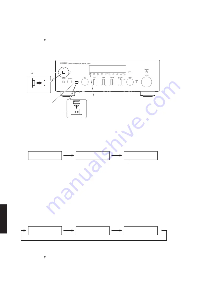
"   " (Power) key

USB jack

USB storage device

"DIMMER" key

Fig. 1

 Operation 

Procedures

*

  Disconnect the power cable of this unit from the AC outlet.

1.  Press the “ ” (Power) key to the ON position. (Fig. 1)

2.  Insert the USB storage device to the USB jack. (Fig. 1)

3.  While pressing the “DIMMER” key, connect the power cable to the AC outlet. (Fig. 1)

4.  The USB UPDATE mode is activated and “USB UPDATE” is displayed. Writing of the firmware starts automatically. 

(Fig. 2)

5.  When writing of the firmware is completed, “UPDATE SUCCESS”, “PLEASE...” and “POWER OFF!” are displayed 

repeatedly. (Fig. 3)

*

  If “ERROR! xxxx” is displayed during writing of the firmware, refer to “List of Error Messages” to determine the 

cause and perform the updating procedure again from the beginning.

Fig. 2

Writing is started.

Writing being executed.

Writing is completed.

Fig. 3


    U S B   U P D A T E


U P D A T E   S U C C E S S


V E R I F Y I N G . . .


P L E A S E . . .


S x - x : x x %


P O W E R   O F F !

S1: NET (IC951/IC953 on DIGITAL P.C.B.) section
S2: MAIN (IC21 on DIGITAL P.C.B.) section
S3: (Not for service)
S4: (Not for service)
S5: (Not for service)

6.  Press the “ ” (Power) key to turn off the power. (Fig. 1)

7.  Remove the USB storage device from the USB jack. (Fig. 1)

8.  Start up the self-diagnostic function and check that the firmware version and checksum are the same as written 

ones. (For details, refer to “Confirmation of firmware version and checksum”)

14

R-N500

R-N50

0

Summary of Contents for R-N500

Page 1: ...chnical capabilities or establish a principle agent relationship of any form The data provided is believed to be accurate and applicable to the unit s indicated on the cover The research engineering a...

Page 2: ...impedance should be equivalent to 1500 ohms shunted by 0 15 F TO SERVICE PERSONNEL Leakage current must not exceed 0 5mA Be sure to test for leakage with the AC plug in both polarities WARNING CHEMIC...

Page 3: ...FRONT PANEL REAR PANELS U C models R S models 3 R N500 R N500...

Page 4: ...K model A model B G models 4 R N500 R N500...

Page 5: ...L model 5 R N500 R N500...

Page 6: ...ce 1 kHz 200 mV CD etc input REC OUT 200 mV 1 0 k ohms SUBWOOFER OUT 4 0 V 1 2 k ohms Cut off frequency 90 Hz Headphone jack 8 ohms load 410 mV 470 ohms Frequency Response CD etc 20 Hz to 20 kHz 0 0 5...

Page 7: ...87 mm 17 1 8 x 5 7 8 x 15 1 4 Weight 9 8 kg 21 6 lbs U U S A model C Canadian model R General model K Korean model A Australian model B British model G European model L Singapore model S Brazilian mod...

Page 8: ...435 17 1 8 151 5 7 8 130 5 1 8 21 7 8 60 Top view Front view 387 15 1 4 340 5 13 3 8 26 1 20 5 3 4 231 9 1 8 54 2 1 8 55 5 2 1 4 335 13 1 4 50 2 DIMENSIONS Unit mm inch 8 R N500 R N500...

Page 9: ...ctricity The time required for discharging is about 30 seconds per each C2044 and C2045 on MAIN 1 P C B C5407 on OPERATION 2 P C B For details refer to PRINTED CIRCUIT BOARDS OPERATION 2 P C B MAIN 3...

Page 10: ...the order as numbered Disconnect the power cable from the AC outlet 1 Removal of Top Cover a Remove 4 screws 4 screws and screw Fig 1 b Remove the top cover Fig 1 2 Removal of Front Panel Unit a Remo...

Page 11: ...ub chassis Unit a Remove 2 screws Fig 2 b Remove CB21 CB61 CB426 CB461 CB463 and CB952 Fig 2 c Unlock and remove CB205 Fig 1 d Remove the sub chassis unit Fig 2 4 Removal of DIGITAL P C B a Remove scr...

Page 12: ...sheet and cloth Bottom cover Power transistor of MAIN 1 P C B and its periphery When checking the MAIN 1 P C B Spread the rubber sheet and the cloth Then place this unit on the cloth upside down Fig...

Page 13: ...tting information soundfield parameters system memory and tuner presetting etc properly Start up the self diagnostic function and select S1 FACTORY PRESET menu For details refer to SELF DIAGNOSTIC FUN...

Page 14: ...ed during writing of the firmware refer to List of Error Messages to determine the cause and perform the updating procedure again from the beginning Fig 2 Writing is started Writing being executed Wri...

Page 15: ...icroprocessor 0100 DSP2 checksum error 0200 DSP2 date reception time out 0400 DSP2 checksum calculation time out Not for service 0800 OSD Flash ROM clearing error OSD Flash ROM failure Malfunction of...

Page 16: ...t for service 5 LINE NOISE 10 MDI Not for service 6 LINE NOISE 10 MDIX Not for service 7 LINK CHECK 8 EXT TEST C Communication system C1 ACCESS CHECK 1 ALL 2 BUS DIR 3 EEPROM 4 TUNER C2 NETWORK IC CHE...

Page 17: ...LEVEL T Troubleshooting Information T1 TROUBLE SHOOTING INFORMATION 1 OPERATING TIME 2 POWER RELAY ON 3 POWER AMP B 4 OUTPUT LEVEL 5 NRC Net Restart Counter Not for service S System and version system...

Page 18: ...keep pressing those 2 keys for 3 seconds or longer The self diagnostic function mode is activated with the protection functions disabled In this mode the SLEEP segment of the FL display flashes to ind...

Page 19: ...oltage across the emitter resistors for each channel Cause An excessive current flowed through the power amplifier Supplementary information As current of the power amplifier is detected the abnormal...

Page 20: ...ion to work in 5 seconds and the power supply will be shut off 2 2 When the protection function worked due to abnormal DC output Cause The voltage in the power supply section is abnormal Supplementary...

Page 21: ...ive heatsink temperature History of protection function When the protection function has worked its history is stored in memory as backup data Even if no abnormality is noted while servicing the unit...

Page 22: ...mode In addition to the self diagnostic function menu items functions listed below are available Power ON OFF Master volume Muting Input selection Functions related to the tuner and the set menu are n...

Page 23: ...el 51 pin on IC21 A 1 2 P R E M U T E A 1 1 N O R M A L A1 3 VOL MUTE The sound signal output is muted inside of IC431 Selector and E Volume IC A 1 3 V O L M U T E A1 4 AC B HIGH Not for service A1 5...

Page 24: ...Normal Short Segment conditions of the FL tube is checked by turning ON and OFF all segments Next a short between segments next to each other is checked by turning ON and OFF all segments alternately...

Page 25: ...connected N1 NETWORK This menu is used to check functions related to NETWORK Connect between LAN port of broadband router and NETWORK jack of this unit with a network cable When the network condition...

Page 26: ...K This menu is used to check that the broadband router is connected correctly N 1 8 E X T T E S T O K OK Normal NG Abnormal Checking N1 8 EXT TEST Transmission reception of the NETWORK port is checked...

Page 27: ...R B U S O K C1 2 BUS DIR Communication and bus line connection between microprocessor IC21 and DIR IC61 are checked OK No error detected NG An error is detected Checking C 1 3 E E P R O M O K C 1 4 T...

Page 28: ...ion between network microprocessor IC21 and SDRAM IC952 are checked C2 3 PHY Ethernet PHYceiver TEST The perform a loopback test in PHY IC955 C2 4 APL Apple ID CHECK Apple authentication IC IC956 devi...

Page 29: ...t is detected The voltage at 120 pin DC_PRT of IC21 is displayed Normal value 38 to 156 Reference voltage 3 3 V 255 If DC becomes out of the normal value range the protection function works to turn of...

Page 30: ...on works to turn off the power THM3 THM2 Not for service THM1 P 1 4 O U T L V L 2 5 5 P1 4 OUTPUT LEVEL Output level of speaker output is detected The voltage at 121 pin AMP_OLV of IC21 is displayed R...

Page 31: ...KEY menu is selected keys become inoperable due to detection of the values of all keys However it is possible to advance to the next menu by turning the VOLUME knob Reference voltage 3 3 V 255 P 1 7...

Page 32: ...r t P 2 2 1 P P O R T P 2 3 1 I N P U T 0 x 0 4 P 2 4 1 V O L d B P 2 7 2 I N P U T 0 x 0 4 P 2 6 2 P P O R T O x 2 E P 2 8 2 V O L d B P 2 9 3 D c 0 0 0 L P 2 1 0 3 P P O R T O x 2 E P 2 1 1 3 I N P...

Page 33: ...g the RETURN key T1 3 POWER AMP B The operation frequency of the POWER AMP B relay RY204 is displayed in hexadecimal notation The operation frequency will be erased by pressing the RETURN key T1 4 OUT...

Page 34: ...because setting to the PRESET RESERVED will cause the user memory content to be erased S2 ROM VERSION CHECKSUM The firmware version and checksum values are displayed The checksum is obtained by addin...

Page 35: ...name and destination S4 1 MODEL DESTINATION The model name and destination are displayed S 4 1 N 5 0 0 0 U 0 2 7 S 4 2 V e r i f y 2 5 5 0 0 S4 2 VERIFY Not for service Not for service Destination U...

Page 36: ...e Attention If the measured voltage exceeds 2 5 mV after repairing the power amplifier check other parts again for any possible defect before removing the resistor 3 Confirm that the voltage is within...

Page 37: ...22 18G 21 17G 20 16G 19 15G 18 14G 17 13G 16 12G 15 11G 14 10G 13 9G 12 8G 11 7G 10 6G 9 5G 8 4G 7 3G 6 2G 5 1G 4 NP 3 NP 36 P30 35 P31 2 1 F1 NX Connection PIN CONNECTION GRID ASSIGNMENT 2G 1G 3G 4G...

Page 38: ...r 1r 1r S4 1 3 P12 1p 1p 1p 1g 2 3 P13 1n 1n 1n 2g 3 3 P14 1d 1d 1d 1f 4 3 P15 2a 2a 2a 2f 5 3 P16 2h 2h 2h 1b 1 4 P17 2j 2j 2j 2b 2 4 P18 2k 2k 2k 1a 3 4 P19 2b 2b 2b 2a 4 4 P20 2f 2f 2f 5 4 P21 2m 2...

Page 39: ...SS AV2 CTRL0 J AV3CLK AV2 DATA1 MEMCKE VSS VSS VSS VSS VSS VSS NC K AV3 CTRL1 AV3 DATA0 NWAIT VSS VSS VSS VSS VSS VSS VSS12 USB L AV2 DATA0 AV3 CTRL0 D0 VSS VSS VSS VSS VSS VSS LCDD5 M D4 VSS VSS VSS...

Page 40: ...ts Master clock output Pin No Function Name I O Detail of Function P4 R3 AV2DATA 3 0 I O Audio data T2 Several formats are supported U1 R1 AV2CLK I O Data clock Depending on the AV Port 2 configuratio...

Page 41: ...Address output SDRAM Bank select F18 A16_BA1 O SRAM Address output SDRAM Bank select G15 A17_DQM0 O SRAM Address output SDRAM Data mask G16 A18_DQM1 O SRAM Address output SDRAM Data mask H17 H16 H15...

Page 42: ...Name I O Detail of Function T17 T16 T15 R17 FD 7 0 I O Bi directional data bus R16 R15 P16 P15 V18 FALE O Address latch enable pull up down defines boot mode U16 FCLE O Command latch enable pull up d...

Page 43: ...onnection Leave this pin open circuit E1 VSS33RTC Power Ground 0 V for RTC Pin No Function Name I O Detail of Function D6 NRES12REF I Voltage reference input NRES12OUT is release when this input volta...

Page 44: ...be left unconnected 18x A4 A5 B4 B5 C8 C9 Pin No Function Name I O Detail of Function J2 VCO 1 0 I External oscillator inputs typically coming from an external VCO Together with the external loop filt...

Page 45: ...L6 L7 L8 L9 L10 L11 L12 L13 M6 M7 M8 M9 M10 VSS Ground 0 V M11 M12 M13 N6 N7 N8 N9 N10 N11 N12 N13 B6 C6 R10 VPP A2 VDD33USB B2 Power supply 3 3 V for USB interface A3 VSS33USB Ground 0 V B3 F3 VDD33P...

Page 46: ...s M16C 60 series Microprocessor core R0L R0H R1H R1L R2 R3 FB A1 A0 R5F3651TNFC IC21 P1_0 P0_7 P0_6 AN0_5 AN0_4 AN0_3 AN0_2 AN0_1 AN0_0 P11_7 P11_6 P11_5 P11_4 P11_3 P11_2 P11_1 P11_0 AN7 AN6 AN5 AN4...

Page 47: ...INT TMR I O I DIR interrupt input 27 P8_0 DRCT_LED O O O O 28 P7_7 DIR_N_RST O O O O DIR reset UART5 unusable because CEC function is used 29 P7_6 DIR_N_CS O O O O DIR chip select UART5 unusable becau...

Page 48: ...rotary encoder A 76 P3_4 FLD_N_CS O O O O FL driver chip select 77 P3_3 FLD_N_RST O O O O FL driver reset 78 P3_2 MIC_N_DET I I I I MIC detection L MIC detected 79 P3_1 STBY_LED O O O O Standby throu...

Page 49: ...etection 122 AN5 THM1 AD I I I Temperature detection 1 123 AN4 THM2 AD I I I 124 AN3 KEY2 AD I I I KEY AD value uptake 2 125 AN2 KEY1 AD I I I KEY AD value uptake 1 126 AN1 PS1_PRT AD I I I PS protect...

Page 50: ...10 RECL2 RECR2 RECL1 RECR1 OUTFL OUTFR SCK SDO WCK BCK NET R NET L IC21 Microprocessor M16C 65 R5F3651TNFC ROM 768kB RAM 47kB RXIN0 RXIN1 RXIN2 RXIN3 NCPU_SCK SDO WCK BCK MPIO_B 0 3 INL8 INR8 A D I DC...

Page 51: ...work Microprocessor IC951 Q2023 12A Ope amp Relay OPE C2036 D2016 C2037 OPE IC44 12A Ope amp Relay 5D P C B MAIN Optical In 25mA x 2 Coax In Buffer Q2024 7A Electronic Volume Q605 5USB iPod iPad USB p...

Page 52: ...OPERATION 8 OPERATION 7 OPERATION 2 OPERATION 2 OPERATION 6 OPERATION 6 OPERATION 8 OPERATION 2 OPERATION 4 OPERATION 3 OPERATION 5 OPERATION 4 OPERATION 3 OPERATION 1 MAIN 7 MAIN 10 MAIN 6 MAIN 3 MA...

Page 53: ...Q201A W2001 CB263 CB264 W2601 CB263 CB264 W2601 MAIN 6 MAIN 2 Wire connection and treatment Apply silicon grease 3 spot Solder these leads of transistor 12 spot Stick damper on the bottom side of MAIN...

Page 54: ...48 37 4 5 1 8 4 5 1 8 1 1 4 5 8 1 28 56 29 2 3 4 NETWORK 1 27 54 1 3 5 4 28 DGND FLD_MOSI FLD_SCK STBY_LED KEY1 REM_IN FLD_N_RST 3 3M MIC_N_DET REC_SEL PSW_N_DET KEY2 VOL_RB 3 3DSP VOL_RA FLD_N_CS IN_...

Page 55: ...IC71 IC954 DIGITAL Side B 1 4 8 5 1 27 54 28 A B C D E F G H I J 1 2 3 4 5 6 7 R N500 55 Semiconductor Location Ref no Location IC71 D5 IC954 H3 Q202 D5 Q203 D4 Q204 D4 Q205 D5 Q206 D5...

Page 56: ...IN_RC IN_RD 3 3DSP DGND IN_RC IN_RD PD_LED DGND DGND 3 3DSP VOL_RA VOL_RB IN_RC DRCT_LED MAIN 5 CB274 MAIN 1 CB205 MAIN 8 CB276 MAIN 7 CB275 PSW_DET 3 3MS 3 3M Z2_LED SELECT PUSH ENTER F2 VP F1 DGND...

Page 57: ...C D E F G H I J 1 2 3 4 5 6 7 R N500 57 Semiconductor Location Ref no Location D4001 I3 D4002 I3 D4003 F4 D4004 F4 D4005 C6 D4006 C6 D4007 I5 D4008 I5 D4010 H3 D4011 G3 D4012 G3 Ref no Location D4013...

Page 58: ...G H I J 1 2 3 4 5 6 7 58 R N500 Safety measures Some internal parts in this product contain high voltages and are dangerous Be sure to take safety measures during servicing such as wearing insulating...

Page 59: ...1 80 40 41 20 21 61 60 1 4 8 5 K A B G L models A B C D E F G H I J 1 2 3 4 5 6 7 R N500 59 Ref no Location D4301 G3 D4302 G3 D4303 G5 D4304 G5 D5402 D3 D5403 C3 D5405 C6 D5406 C6 D5407 C6 D5408 C6 D...

Page 60: ...NETR NETE AE PS2_PRT 5A NETE CD_E CD_L CD_R NC TUE TUL NETE NETL AE NETR IN OUT COM 12A NETE PS2_PRT CD_R NC CD_L CD_E TUR AV2_D TUE AV1_D 5A 5DSP TUR TUL AV3_D DGND AE AV4_D DGND NETL NETE NETR SCL N...

Page 61: ...ON 4 Side B OPERATION 5 Side B OPERATION 6 Side B 1 7 14 8 4 5 8 1 K B G L models A B C D E F G H I J 1 2 3 4 5 6 7 R N500 61 Semiconductor Location Ref no Location D4351 D4 D4401 G3 IC436 C3 IC461 H6...

Page 62: ...ION 8 Side A PHONES MAIN 1 W2004 DIGITAL CB61 DIGITAL CB952 OPERATION 6 CB462 HPR HPE HP_N_DET HPL HPE 5USB 5USB GND GND FG DGND Vreturn DATA DATA USB jack LOL VOL VOR AGND LOR LOL VOL VOR AGND LOR LO...

Page 63: ...C466 OPERATION 7 Side B 1 4 8 5 OPERATION 10 Side B OPERATION 11 Side B OPERATION 8 Side B A B C D E F G H I J 1 2 3 4 5 6 7 R N500 63 Semiconductor Location Ref no Location D4261 C5 D4262 C5 IC466 C4...

Page 64: ...S models Note Those parts marked with are not included in the P C B assembly B C E B C E B C E B C E Q201A Q201C Q202A Q202C A B C D E F G H I J 1 2 3 4 5 6 7 64 R N500 Semiconductor Location Safety...

Page 65: ...o Location D2001 C4 D2002 C5 D2003 H5 D2004 H4 D2005 D5 D2006 D3 D2007 E3 D2008 H6 D2009 E5 D2012 E6 D2013 D6 D2017 D4 D2018 F4 D2021 G7 D2023 D4 D2024 F4 D2027 H3 IC201 G2 Q2001 C4 Q2002 C5 Q2005 C4...

Page 66: ...ND 5 5V 5 5V 5 5V GND GND PRY DGND ACPWR_DET 3 3M CPU_N_RST DEST 3 3MS 3 3M PSW_DET FRST FRST 5 5V GND GND 5 5V GND THM3_PRT SPRY_5CH NET_RE NC MUTE_SW PS1_PRT PDSW NET_RF NC DC_PRT I_PRT VOL_MOSI AMP...

Page 67: ...N 2 Side B MAIN 3 Side B MAIN 4 Side B MAIN 5 R S models A B C D E F G H I J 1 2 3 4 5 6 7 R N500 67 Ref no Location D2781 D7 D2782 C6 D2783 B6 D2784 B6 D2785 B6 Q2781 B6 Q2782 D6 Q2783 B6 Semiconduct...

Page 68: ...MAIN 8 MAIN 2 W2601 VCC OUT GND OPERATION 1 CB404 DIGITAL CB65 OPERATION 1 CB407 THM1_PRT DGND 3 3S 3 3DSP DGND VOL_RA VOL_RB VOLUME PD_LED DGND 3 3DSP 5EX DGND DGND 5EX PURE DIRECT indicator DC OUT A...

Page 69: ...Side B MAIN 6 Side B MAIN 7 Side B Side B Side B MAIN 8 MAIN 9 MAIN 10 A B C D E F G H I J 1 2 3 4 5 6 7 R N500 69 Ref no Location Q2751 H3 Semiconductor Location...

Page 70: ...7 5B UDZV30B UDZV39B 1N4003S 1SS355VMTE 17 RS203M B C J80 DBL155G RF101L2STE25 RB215T 90 SARS05 RS603M B C J80 8 4 1 8 4 1 65 102 38 1 103 128 64 39 48 13 37 24 1 12 36 25 8 4 1 8 4 1 1 10 20 3 1 5 4...

Page 71: ...B01JE TE85L B1 E B2 C2 C1 P L 3 0 N C P U _ A M U T E 3 3M 3 3M 3 3S 3 3 S 3 3S 3 3 S 3 3 S 3 3 S 3 3M 3 3M 3 3M 3 3M 3 3M 3 3M 3 3H 3 3DSP 3 3M 3 3S 3 3S 3 3S 3 3M 3 3M 3 3M 3 3S 5 T 3 3 M 3 3 D S P...

Page 72: ...2 7 A X R 0 9 A X R 1 4 S P I 1 _ S I M O 1 2 8 C V D D 1 2 9 V S S 1 3 0 A X R 0 1 0 A X R 1 3 1 3 1 A X R 0 1 1 A X R 1 2 1 3 2 C V D D 1 3 3 V S S 1 3 4 A X R 0 1 2 A X R 1 1 1 3 5 A X R 0 1 3 A X...

Page 73: ...609 no_use 1 2 3 4 5 6 R 6 6 5 n o _ u s e Q 6 0 8 n o _ u s e 3 3D DAB_PON RP130Q331D TR F YC288A0 IC69 4 V D D 2 G N D 3 V O U T 1 C E C E 5A NGND C 6 8 0 1 0 6 3 C 6 7 9 1 0 1 0 R 6 6 7 4 7 K R 7 0...

Page 74: ...C10 SSMCLK D12 SSMD7 C12 SSMD6 B12 SSMD5 A12 SSMD4 D11 SSMD3 C11 SSMD2 A5 NC B5 NC A4 NC B4 NC B11 SSMD1 A11 SSMD0 V9 LCDCTRL3 U9 LCDCTRL2 T9 LCDCTRL1 R9 LCDCTRL0 T10 LCDCLK B7 NC C9 NC C8 CN U4 LCDD...

Page 75: ...4 C 0 C B 4 2 7 1 2 3 4 D 4 0 0 1 1 S S 3 5 5 V M R4006 1K J4001 R4005 1K C4029 0 1 16 R4016 2 2K W4001 no_use C 4 0 1 9 2 2 0 P S L D 4 0 0 8 1 S S 3 5 5 V M C4026 0 1 16 W4002 no_use R 4 0 3 9 0 FG...

Page 76: ...41 KIA7805API OUT COM IN D4401 1SS355VM C 4 4 0 1 1 0 5 0 R4401 1P22 S T 4 4 1 R4331 1P22 Q4301 C4488 S T R 4 3 2 6 1 8 K R 4 3 3 0 1 K 7A 12A C 4 3 2 2 1 0 5 0 D 4 3 0 1 U D Z V 7 5 B R4332 1P22 R 4...

Page 77: ...M CB542 C5402 1000P 250 R 5 4 1 6 8 2 K R5407 1P47 FI541 ELF17N010AK 1 4 3 2 ST541 C 5 4 0 1 s 5 4 2 C 5 4 0 7 s 5 4 3 C5411 s545 C5412 s542 F5402 s541 R5418 s544 CB545 53290 0880 CB546 53290 0480 C 5...

Page 78: ...B D 2 0 0 7 U D Z V 5 1 B D 2 0 2 0 n o _ u s e Q2029 no_use D 2 0 2 1 U D Z V 3 9 B R 2 0 8 0 4 7 R 2 0 8 2 4 7 4 7 R2045 4 7 R2042 4 7 R2043 4 7 R2044 R2038 4 7 R2037 4 7 2 7 K R 2 0 3 6 2 7 K R 2 0...

Page 79: ...PLAY FLTR CE CERAMIC FILTER FLTR COMB COMB FILTER MODULE FLTR LC RF LC FILTER EMI FUSE CHP CHIP FUSE GND MTL GROUND PLATE GND TERM GROUND TERMINAL JUMPER CN JUMPER CONNECTOR JUMPER TST JUMPER TEST POI...

Page 80: ...F 16V C621 UB214680 C CE CHP 0 068uF 25V C622 US643470 C CE CHP 4700pF 25V C623 US625100 C CE CHP 0 1uF 10V C624 WD758300 C CE CHP 10uF 10V C625 US625100 C CE CHP 0 1uF 10V C626 US663100 C CE CHP 1000...

Page 81: ...N 14P CB444 VQ963600 CN BS PIN 15P CB461 VB858400 CN BS PIN 5P CB462 VQ044300 CN BS PIN 7P CB463 VB858500 CN BS PIN 6P CB466 VQ047100 CN BS PIN 7P CB469 VK026400 CN BS PIN 5P CB541 VG879900 CN BS PIN...

Page 82: ...4302 WY163600 DIODE ZENR UDZV7 5B D4303 4304 WW783900 DIODE 1SS355VM D4351 WY163300 DIODE ZENR UDZV5 6B D4401 WW783900 DIODE 1SS355VM D5401 WW872000 DIODE BRG DBL155G 1 5A 600 D5402 WE665600 DIODE RF1...

Page 83: ...LAR 0 39uF 50V C2049 2050 WJ610600 C MYLAR 0 022uF 100V C2051 VR168300 C MYLAR 0 1uF 50V C2052 UR268100 C EL 100uF 50V C2054 2055 US135100 C CE CHP 0 1uF 16V C2056 2057 UR237470 C EL 47uF 16V C2058 UR...

Page 84: ...L005390 R MTL OXD 390 1 2W R2030 2031 HL005820 R MTL OXD 820 1 2W R2032 HL005390 R MTL OXD 390 1 2W R2033 WW865300 R CAR FP 2 7K 1 4W R2034 2035 HL006100 R MTL OXD 1K 1 2W R2036 WW865300 R CAR FP 2 7K...

Page 85: ...3220 HF85 3220 3 3 HJ35 3330 HF85 3330 4 7 HJ35 3470 HF85 3470 5 6 HJ35 3560 HF85 3560 10 HF45 4100 HF45 4100 15 HJ35 4150 HF85 4150 22 HF45 4220 HF45 4220 27 HJ35 4270 HF85 4270 33 HF45 4330 HF45 43...

Page 86: ...0 110 129 129 129 133 123 123 123 103 129 129 125 183 129 101 172 120 175 175 174 122 122 125 129 132 132 182 125 123 123 150 124 124 117 103 120 120 120 120 127 120 173 2 6 1 3 4 2 9 4 2 4 4 2 3 6 1...

Page 87: ...B TONE CONTROL SI 114 ZJ461100 CAP POWER BL 114 ZJ461000 CAP POWER SI 115 ZG193100 KNOB SELECT BL 115 ZG193000 KNOB SELECT SI 116 WU966400 CAP DIRECT BL Ref No Part No Description Remarks Markets Ref...

Page 88: ...0 SIDE PLATE SI 5 6 WW649200 SUPPORT LENS DIRECT 5 7 ZG192800 WINDOW SHEET 5 11 WK863700 LENS RC PURPLE BL 5 11 WK863600 LENS RC MEDIUM SI 6 1 ZH227800 P C B ASSEMBLY OPERATION U 6 1 ZH227900 P C B AS...

Page 89: ...2x10x170 4 1 7 WE774200 BIND HEAD B TIGHT SCREW 3x10 MFZN2W3 4 2 ZH227400 P C B ASSEMBLY MAIN UCA 4 2 ZH227500 P C B ASSEMBLY MAIN RS 4 2 ZH227600 P C B ASSEMBLY MAIN KBGL 4 3 MF121100 FLEXIBLE FLAT...

Page 90: ...79 75 76 66 70 73 69 68 67 71 72 62 58 61 65 64 63 59 60 48 51 54 50 49 52 53 44 40 47 46 45 42 24 27 31 30 29 25 26 38 16 20 19 18 17 12 8 11 15 14 SW2 3 2 1 9 0 10 TV VOL ENT TV TV CH 6 7 8 4 3 2 5...

Page 91: ...7F01 720C Switch to DEVICE mode go to USB page 23 NET 7F01 3F 7F01 3FC1 Switch to DEVICE mode go to NET page 24 FM 7F01 5827 7F01 5826 25 AM 7F01 552A 7F01 552B 26 PRESET 7F01 5B24 7F01 5B25 27 TUNING...

Page 92: ...EIVER 55 TOP MENU 7A A0DF 7A A0DE 56 POP UP MENU 7A A4DB 7A A4DA 57 MUTE 7A 1C 7A 1CE2 RECEIVER RECEIVER 58 DISK SKIP 7986 4FB0 7986 4FB0 7C83 8B74 7C83 8B74 7986 4FB0 59 STOP 7F01 69 7F01 6997 7C83 8...

Page 93: ...n input sources Signal Info Displays information about the audio signal Auto Preset Automatically registers FM radio stations with strong signals as presets Clear Preset TrafficProgram Clear radio sta...

Page 94: ...e network parameters such as IP address MAC Filter Filter Sets the MAC address filter to limit access to the unit from other network devices DMC Control Selects whether to allow a DLNA compatible Digi...

Page 95: ...l playback of the unit from DMCs such as Windows Media Player 12 on the same network NET Standby Selects whether the unit can be turned on from other network devices network standby Network Setup NewF...

Page 96: ...d then countdown starts in the front display Enables disables the eco power saving mode When the eco mode is enabled you can reduce the unit s power consumption Be sure to press ENTER to restart the u...

Page 97: ...down numeric key 1 for more than 3 seconds To select ID2 while holding down the ID hold down numeric key 2 for more than 3 seconds Once the remote control code is successfully registered Rem Success a...

Page 98: ...TER repeatedly to select USB or NETWORK and press DISPLAY to start firmware update Choices If the unit detects newer firmware over the network NewFwAvailable appears as the Information menu item in Ne...

Page 99: ...99 R N500 R N500 MEMO...

Page 100: ...R N500...

Reviews: