


A
1
2
3
4
5
6
7
8
9
10
B
C
D
E
F
G
H
I
J
K
L
M
N
RX-E810/RX-E410/NX-E800
37
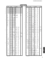
★
All voltages are measured with a 10M
Ω
/V DC electronic volt meter.
★
Components having special characteristics are marked
s
and must be replaced
with parts having specifications equal to those originally installed.
★
Schematic diagram is subject to change without notice.
INPUT
4.7
0
6.1
6.1
4.7
0
0
10.5
11.2
11.2
11.2
10.3
10.3
0
0
0
11.2
11.2
0.1
0
0
0
0
0
0
0
0
0
0
0
0
0
0
0
0
0
11.2
-11.0
9.6
10.3
5.5 5.5
4.9
4.9
4.7
5.5
5.5
4.7
0
0
0
0
0
0
0
0
0.3
4.7
4.7
0
0
0
0
0
0
0
0
0
0
0
0
0
0
0.4
0
0
0
0
0
0
0
0
0
0
0
4.7
4.9
4.8
4.8
0
4.8
4.9
4.7
4.7
0
0
0
0.1
2.5
2.5
0
4.9
4.9
4.9
11.2
-11.1
-18.7
-12.4
-12.4
0
0
0
-12.4
-18.7
-18.7
18.4
18.4
12.5
12.5
18.4
-18.7
0
0
12.5
-11.0
2.5
3
a
b
AC 4.5
AC 28.4
INPUT L
RX-E810
RX-E410
INPUT (2)
INPUT (1)
POWER TRANSFORMER
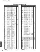
IC200
: M30620MCP-A41FP
Single-chip 16-bit cmos microcomputer
Output (timer A): 5
Input (timer B): 6
Internal peripheral functions
Watchdog timer
(15 bits)
DMAC
(2 channels)
D/A converter
(8 bits X 2 channels)
Memory
ROM
128K
RAM
10K
A/D converter
(10 bits
X
8 channels
Expandable up to 26 channels)
UART or
clock synchronous serial I/O
(8 bits
X
3 channels)
System clock
generation circuit
XIN-XOUT
XCIN-XCOUT
PLL frequency synthesizer
On-chip oscillator
M16C/60 series16-bit CPU core
Port P0
8
Port P1
8
Port P2
8
8
8
8
Port P6
8
8
R0L
R0H
R1H
R1L
R2
R3
A0
A1
FB
SB
ISP
USP
INTB
CRC arithmetic circuit (CCITT )
(Polynomial : X
16
+X
12
+X
5
+1)
Multiplier
7
8
8
P
or
t P10
Po
rt
P
9
P
o
rt
P8_5
P
or
t P8
P
or
t P7
Port P5
Port P4
Port P3
Clock synchronous serial I/O
(8 bits
X
2 channels)
PC
FLG
Timer (16-bit)
Three-phase motor
control circuit
<VCC2 ports>
(4)
<VCC1 ports>
<VCC1 por
ts>
IC201
: NJM2068MD-TE2
Dual operational amplifier
–
+
OUT
1
–IN
1
–V
CC
+V
CC
OUT
2
1
2
3
4
5
+IN
1
–IN
2
+IN
2
–
+
6
7
8
IC202
: LC78211
Analog function switch
1
2
3
4
5
6
7
8
9
10
11
30
29
28
27
26
25
24
23
22
21
20
19
16
12
18
17
14
15
13
LEVEL SHIFTER
LATCH
CONTR
O
L
SHIFT REGISTER
ZZ
ZZ
ZZ
L1
L2
L3
L4
LCOM1
L5
L6
L7
L8
RES
S
V
DD
V
SS
V
EE
LCOM2
LCOM3
R1
R2
R3
R4
RCOM1
RCOM2
RCOM3
R5
R7
R8
D1
CL
CE
R6
IC203
: LC72722PM
RDS signal processor
REFERENCE
VOLTAGE
57 kHz
bpf
(SCF)
CCB
TEST
PLL
(57 kHz)
ANTIALIASING
FILTER
SMOOTHING
FILTER
RAM
(24 BLOCK DATA)
ERROR CORRECTION
(SOFT DECISION)
SYNC / EC
CONTROLLER
SYNC
DETECT-1
DATA
DECODER
CLOCK
RECOVERY
(1187.5 Hz)
MEMORY
CONTROL
OSC/DIVIDER
VREF
CLK (4.332 MHz)
SYNC
DETECT-2
VDDA
VSSD
VDDD
RDS-ID
SYNC
SYR
VSSA
MPX IN
DO
CL
DI
CE
T1
T2
T3
T4
T5
T6
T7
X IN
VREF
FL OUT
C IN
X OUT
3
14
15
19
18
24
1
5
6
4
2
20
21
22
23
7
8
9
10
11 16 17
13
12
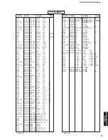
POINT
1 Pin 11 of IC200
POINT
3 a / Pin9, b / Pin8 of CB205
AC cable ON
+5M
/RESET
AC cable OFF
POINT
2 Pin 13 of IC200
AC cable ON
a
a
b
b
to OPEREA
TION (1)_CB501
P
age 33
B9
to MAIN (4)_CB20
P
age 36
G9
to MAIN (1)_CB12
Page 35
D2
to MAIN (4)_CB18
Page 36
G7
to MAIN (2)_W1
Page 36
B2
to OPERATION (2)_CB702
Page 34
L4
to MAIN (1)_CB15
Page 35
G2
to OPERA
TION (1)_W501
P
age 33
I3
to MAIN (1)_CB13
P
age 35
D2
TUNER


