background image

18

DD-55

30

030

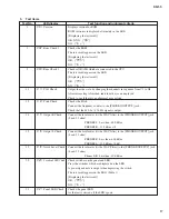
: Pad Check

Checks the PAD.

When a pad is tapped, the LED's indicate its identification number and tapping

power.

[Displaying the test result]

                        Maximum data: 7F

                        Minimum data: 18

31

031

: Pedal 1 Check

Checks the [PEDAL 1].

Connect the pedal to the [PEDAL 1] jack. When the pedal is stepped on, it

sounds in bass drum tones. The LED's indicate the tapping power.

[Displaying the test result]

                        Maximum data: 7F

                        Minimum data: 38

32

032

: Pedal 2 Check

Checks the [PEDAL 2].

Connect the pedal to the [PEDAL 2] jack.

Check that the C3 note is output when starting the test program.

Check that the C4 note is output when pushing the pedal and that tone is turned

off when releasing the pedal.

"20F" is displayed and the sound stops.

37

037

: MIDI Check

Checks the MIDI.

After connecting the [MIDI IN] and [MIDI OUT] with a MIDI cable, execute

the test.

Check that the C4 note is output and the test result appears on the LED.

[Displaying the test result]

OK:  ["

PAS

"]

NG:  ["

Err

"]

41

041

: Rom 2 Check

Checks the ROM.

The test result appears on the LED.

[Displaying the test result]

OK:  ["

PAS

"]

NG:  ["

Err

"]

42

042

: Ram 2 Check

Checks the RAM.

The test result appears on the LED.

[Displaying the test result]

OK:  ["

PAS

"]

NG:  ["

Err

"]

46

046

: Rom Backup

Performs the RAM back-up check.

          Check 2

After checking that the beginning becomes NG, turn the power switch off.

Enter the test program and perform the RAM back-up and check again.

[Displaying the test result]

OK:  ["

PAS

"]

NG:  ["

Err

"]

---: Factory Set

All RAMs are initialized and set to the factory preset date when executing this

test. Set the [STANDBY/ON] switch to ON with the [DEMO] button pressed

and held.

Turn the power off.

Summary of Contents for Druid Pro DD-55

Page 1: ...NEL LAYOUT 4 DIMENSION 5 CIRCUIT BOARD LAYOUT 6 BLOCK DIAGRAM 7 DISASSEMBLY PROCEDURE 8 LSI PIN DISCRIPTION 10 IC BLOCK DIAGRAM 11 CIRCUIT BOARDS 11 TEST PROGRAM 16 MIDI IMPREMENTATION CHART 20 PARTS LIST OVERALL CIRCUIT DIAGRAM This document is printed on chlorine free ECF paper with soy ink PEDAL 1 PEDAL 2 ...

Page 2: ...es in specification are subject to change without notice or obligation to retrofit Should any discrepancy appear to exist please contact the distributor s Service Division WARNING Static discharges can destroy expensive components Discharge any static electricity your body may have accumulated by grounding yourself to the ground bus in the unit heavy gauge black wires connect to this bus IMPORTANT...

Page 3: ...RUM 3 BACKING button DEMO button CLICK but ton START STOP button A B REPEAT button BREAK TAP button REC button DIAL LED Display Song Drum Kit Tempo etc Auxiliary jacks DC IN12 V PHONES OUTPUT MIDI IN OUT PEDAL 1 2 Oouput Impedance 33Ω PHONES OUTPUT jack Main Amplifier 5W 5W EIAJ Speaker 8 cm x 2 Power Consumption 16 W when using PA 5C power adaptor Power Supply Adaptor DC12V Yamaha PA 5C sold sepa...

Page 4: ...dal 2 Pedal 1 0 SONG Button 1 TEMPO Button 2 START STOP Button 3 A B REPEAT Button 4 BREAK TAP Button 5 REC Button 6 STANDBY ON Switch 7 DIAL 8 Drum Pads x7 q DEMO Button w CLICK Button e DISPLAY r VOLUME Buttons t HAND PERC Button y DRUM 1 3 Buttons u BACKING Button i PAD Button o KIT Button ...

Page 5: ...Side Panel L Side Panel R Side Panel Left 9 DC IN 12V AC Adaptor Jack 0 PHONES OUTPUT Jack 1 PEDAL 2 Jack Side Panel Right 2 MIDI IN Terminal 3 MIDI OUT Terminal 4 PEDAL 1 Jack 558mm 173 6mm 166 8mm 354 7mm 362mm DIMENSION ...

Page 6: ...6 DD 55 CIRCUIT BOARD LAYOUT DD 1 2 DD 2 2 Pad Assembly Pad Assembly L Speaker L Speaker R 160 U220 Upper Case Lower Case Top view ...

Page 7: ...37 40 47 48 51 59 62 71 80 87 89 96 99 102 118 121 123 127 131 145 147 150 151 152 IC150 3P 13 16 1 3 4 7 8 1 9 11 6 3 7 2 8 2 7 15 14 32 30 24 24 22 32 11 1 10 14 21 23 30 32 42 2 15 17 21 23 25 28 31 2 15 17 21 23 25 28 31 3 2 IC930 3P IC920 4P IC940 3P TR930 IC190 3P 1 2 1 2 1 3 IC710 11 IC710 5 6 12 13 IC750 5 6 12 13 IC790 5 6 12 13 IC710 8 IC710 4 IC710 1 IC750 11 IC750 8 IC750 4 IC750 1 GAT...

Page 8: ... can then be removed Fig 5 When removing the lower case pay attention not to break 160 BAT bundled cables see Fig 2 When working with the unit turned over place it on a soft cloth to protect the surface from scratches 80 Binding Head Tapping Screw B 3 0X12 MFZN2BL VQ074600 3 DD 1 2 Circuit Board Time required about 4 min 3 1 Remove the lower case assembly See procedure 1 3 2 Remove the DD 2 2 circ...

Page 9: ...e procedure 3 4 4 Pull a pad assembly off the panel as shown in the illustration Fig 7 The pad assembly S and pad assembly L can then be removed in the same manner 5 Speakers Time required about 3 min 5 1 Remove the lower case assembly See procedure 1 5 2 Remove the four 4 screws marked 135 The speakers can then be removed Fig 6 The left speaker and right speaker can then be removed in the same ma...

Page 10: ...ve memory data bus 122 CMD15 I O Program memory Data bus 39 SMD0 I O 123 CMD0 I O 40 SMD15 I O 124 CMA21 O Program address bus 41 SOE O read signal 125 PDT15 I O 42 SWE O write signal 126 PDT14 I O 43 SRAS O RAS signal 127 PDT13 I O 44 SCAS O CAS signal 128 PDT12 I O SWX access data bus 45 REFRESH O REFRESH signal 129 PDT11 I O 46 CS0 O CS signal 130 PDT10 I O 47 SMA0 O Memory address bus 131 PDT9...

Page 11: ...A GND Analog ground 13 WDCK I Word clock 6 R OUT O Channel R output 14 RSI I Channel R series input 7 A VDD Analog power supply 15 SI LSI I Series input Channel L series input 8 A VDD 16 CLK I Clock 1 2 3 4 5 6 7 13 12 11 10 9 8 14 1A 1B 2B 2A 2C 3C GND Vcc 1C 4C 4A 4B 3B 3A SN74HC4066NSR XZ824A00 HD74HC4066NSR X0563A00 ANALOG SWITCH 1 A 2 3 4 5 6 7 8 9 V IN V IN OUT V IN IN OUT B uPC4572HA XF633A...

Page 12: ...12 DD 55 A A MIDI IN MIDI OUT PEDAL 1 to DD 2 2 CN460 DD 1 2 Circuit Board Component Side Component Side DD 1 2 2NA V707790 1 ...

Page 13: ...13 DD 55 to Battery to Speaker L R DC IN 12V PHONES OUTPUT PEDAL 2 A A Component Side DD 1 2 2NA V707790 1 ...

Page 14: ...14 DD 55 PAD 1 PAD 2 DEMO CLOCK REC BREAK TAP A B REPEAT START STOP HAND PERC DRUM1 DRUM2 PAD KIT A A DD 1 2 Circuit Board Pattern Side Pattern Side DD 1 2 2NA V707790 1 ...

Page 15: ...15 DD 55 PAD 3 PAD 4 PAD 5 PAD 6 PAD 7 VOLUME BACKING TEMPO DRUM3 DRUM2 SONG KIT STANDBY ON A A Pattern Side DD 1 2 2NA V707790 1 ...

Page 16: ...ds To start a test press the START STOP button Pressing the START STOP button again returns to the selected item If you pass the test and return to the selected item a dot appears on the upper left of the LED segment See Fig 2 If you fail the test the LED shows Err See Fig 3 To return to the selected item press the DEMO button Note that the START STOP button is inactive at this time Even if the te...

Page 17: ...Pitch Connect the frequency counter to the PHONES OUTPUT jack Check that the 440 0 1 76 Hz signal is output 14 014 Output R Check Connect the level meter with a JIS C filter to the PHONES OUTPUT jack Load 33 ohm PHONES L Less than 60 0 dBm PHONES R 11 5 dBm 2 15 015 Output L Check Connect the level meter with a JIS C filter to the PHONES OUTPUT jack Load 33 ohm PHONES R Less than 60 0 dBm PHONES L...

Page 18: ...and the sound stops 37 037 MIDI Check Checks the MIDI After connecting the MIDI IN and MIDI OUT with a MIDI cable execute the test Check that the C4 note is output and the test result appears on the LED Displaying the test result OK PAS NG Err 41 041 Rom 2 Check Checks the ROM The test result appears on the LED Displaying the test result OK PAS NG Err 42 042 Ram 2 Check Checks the RAM The test res...

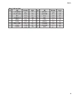
Page 19: ...S01 C2 10 HI HAT S10 A2 2 START STOP S02 C 2 11 BACKING S11 A 2 3 REC S03 D2 12 PAD S12 B2 4 BRAKE TAP S04 D 2 13 KIT S13 C3 5 DEMO S05 E2 14 SONG S14 C 3 6 CLICK S06 F2 15 TEMPO S15 D3 7 HAND PERC S07 F 2 16 VOLUME S16 D 3 8 BASS S08 G2 17 VOLUME S17 E3 9 SNARE S09 G 2 18 DIAL O F3 ...

Page 20: ...usive o 4 o 4 Song Pos x x Common Song Sel x x Tune x x System Clock o o Real Time Commands o o 2 Aux All Sound OFF x o 120 Reset All Cntrls x o 121 Local ON OFF x x All Notes OFF x x Mes Active Sense o o sages Reset x x Mode 1 OMNI ON POLY Mode 2 OMNI ON MONO o Yes Mode 3 OMNI OFF POLY Mode 4 OMNI OFF MONO x No 0 32 o o Bank Select 1 o 3 o Modulation 6 38 o 3 o Data Entry 7 o o Volume 10 o 1 o Pa...

Page 21: ... model 220V I Indonesian model N X General export model J Japanese model Y Export model WARNING Components having special characteristics are marked and must be replaced with parts having specifications equal to those originally installed CONTENTS OVERALL ASSEMBLY 2 ELECTRICAL PARTS 4 The numbers in QTY shows quantities for each unit The parts with in Part No are not available as spare parts The s...

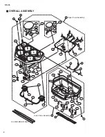
Page 22: ... U20 A B C D E F H H I I G 10 20 50 60 80 30 100 100 160 U100 U130 U135 U135 U110 U220 L110 L100 L100 U200 U210 U140 U10 L10 L50 L30 L40 L60 L80 L80 L70 L90 L90 L20 L20 U40 U95 U50 U80 U70 U60 U90 U10a U10b U10c Upper Case Assembly Lower Case Assembly ACCESSORIES Stick ...

Page 23: ...ly Cushion PN Switch PN Switch PN Switch PN Switch Lens LED Dust Proof Cloth Slider Brush Bind Head Tapping Screw B Bind Head Tapping Screw B Adhesive Tape Circuit Board Speaker Connector Assembly Bottom Case Assembly Bottom Case Spring Terminal Contact Spring Contact Spring Foot Cushion Cushion Cushion Cushion Dust Proof Cloth Dust Proof Cloth Pad L Assembly Pad Rubber Adhesive Tape Piezo Electri...

Page 24: ...uctive Cera Cap Electrolytic Cap Semiconductive Cera Cap Electrolytic Cap Electrolytic Cap Electrolytic Cap Electrolytic Cap Electrolytic Cap Electrolytic Cap Electrolytic Cap Electrolytic Cap Electrolytic Cap Electrolytic Cap Electrolytic Cap Ceramic Capacitor B Electrolytic Cap Electrolytic Cap Ceramic Capacitor B Electrolytic Cap Semiconductive Cera Cap Electrolytic Cap Electrolytic Cap Semicon...

Page 25: ...uctive Cera Cap Electrolytic Cap Semiconductive Cera Cap Electrolytic Cap Semiconductive Cera Cap Electrolytic Cap Electrolytic Cap Semiconductive Cera Cap Electrolytic Cap Semiconductive Cera Cap Semiconductive Cera Cap Ceramic Capacitor Array Cable Holder Cable Holder Base Post Connector Base Post Connector Diode Diode Diode Diode Diode Diode Diode Diode Diode Diode Diode Diode Diode Diode Diode...

Page 26: ...eads Coil Ferrite Beads Coil Ferrite Beads Coil Ferrite Beads Coil Ferrite Beads Coil Ferrite Beads Ferrite Beads Coil Coil Ferrite Beads Ferrite Beads Ferrite Beads Ferrite Beads Ferrite Beads Ferrite Beads Ferrite Beads Ferrite Beads Coil Coil Ferrite Beads Ferrite Beads Ferrite Beads Coil Ferrite Beads Coil Coil LT2A02 E 1SS133 1SS176 1SS133 176 HSS104 11ES4 11ES4 TA1 11ES4 11ES4 TA1 REB161 PVB...

Page 27: ...sistor Carbon Resistor Carbon Resistor Carbon Resistor Carbon Resistor Carbon Resistor Carbon Resistor Carbon Resistor Carbon Resistor Carbon Resistor Carbon Resistor Carbon Resistor Carbon Resistor Carbon Resistor Carbon Resistor Carbon Resistor Carbon Resistor Carbon Resistor Carbon Resistor Carbon Resistor Carbon Resistor Carbon Resistor Carbon Resistor Carbon Resistor Carbon Resistor Carbon Re...

Page 28: ...or Carbon Resistor Carbon Resistor Carbon Resistor Carbon Resistor Carbon Resistor Carbon Resistor Carbon Resistor Carbon Resistor Carbon Resistor Carbon Resistor Carbon Resistor Carbon Resistor Carbon Resistor Carbon Resistor Digital Transistor Digital Transistor Digital Transistor Digital Transistor Transistor Transistor Transistor Transistor Connector Assembly Ceramic Resonator Ceramic Resonato...

Page 29: ...V REGULATOR 5V STANDBY ON ANALOG SWITCH ANALOG SWITCH POWER AMP 28CC1 8819213 28CC1 8819213 1 1 REGULATOR 3 3V PC29M33HF XT333A00 1 2 3 3 OUTPUT 2 COMMON 1 INPUT REGULATOR 5V AN78L05 XM927A00 2 1 3 3 OUTPUT 2 GND 1 INPUT REGULATOR 5V S81250SGY Z XT625A00 2 1 3 3 OUTPUT 2 INPUT 1 GND PQ05RF2 XH672A00 REGULATOR 15V 2 OUT 1 IN 3 GND 4 ON OFcont 4 3 2 1 IC930 IC920 IC190 IC940 DD 55 OVERALL CIRCUIT DI...

Reviews: