background image

7

CLP-970/CLP-970M/CLP-970C/CLP-970A/CLP-970AM/CLP-970AC

 CIRCUIT BOARD LAYOUT

to SP Box Ass'y

to PN Ass'y

to MK Ass'y

to PN Ass'y

CN2

CN1

CN1

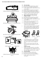
CN1 CN2

CN3

CN1 CN8 CN9 CN5

CN1

CN4

CN2

CN1

CN2

CN6

CN5

CN1

CN3

CN6

CN4

CN7

CN2

CN200

CN220

CN240

CN210

NOTE2

Keyboard

MA120

FDD

PSW

FU120L

NW

PN

DM

A-JACK

D-JACK

34

C

D

31

21

20

19

35

13

36

80

81

A

29

32

30

33

B

H.P

P.L

SWX-XG

SWX-A

SWX-C

SWX-E
SWX-F

E

E

Filament Tape

Code Binder

Ferrite Core

Cable Holder

Connector Direction

Connector Direction

Wire Clamp

Lug Tarminal

Fixed by filament tape
at the side

NOTE1)

NOTE2)

NOTE3)

NOTE4)

NOTE5)

Model equipped with "A" has no floppy disk drive.

FDD unit

81

80

The guide for the cable ass'y 80 shall be fitted downward.
The cable assemblies 80 and 81 shall be loose-fitted as 
shown in the figure below. 

[ Side view ]

The symboles in above drawing described below.

Nut

29 Wire Hamess is fixed by Vinyl Tie (A) so as not to touch Heat Sink.
And fix it by the Filament Tape so that a DM circuit board side may not
become loose.

80,81 Wire Hamess and Cable Holder (B) are not installed.

PARTS LIST REF NO.

CONNECTOR NAM PIN/LENGTH DESTINATION

Speaker Box Assembly [13]

Panel Assembly [19]
Panel Assembly [20]
Panel Assembly [21]

Main Unit [29]
Main Unit [30]
Main Unit [31]
Main Unit [32]
Main Unit [33]
Main Unit [34]
Main Unit [35]
Main Unit [36]
Main Unit [80]
Main Unit [81]

End block Assembly [4]

Main Unit [59]

FLOPPY DISK DRIVE ASSEMBLY [5]

Main Unit [5b]

LOCATION

13
19
20
21
29
30
31
32
33
34
35
36
80
81

A
B

C
D

SP
KRD-KRD
KRD-KRD
VOL
KRD-KRD
KRD-KRD
KRD-KRD
MK-LF
KRD-KRD
KRD-KRD
KRD-KRD
SP1
FDD-SIG
FDD-POW
PSW
GND
GND
KRD-KRD

8P
16P / L=350
15P / L=400
8P /

L=400

7P  / L=450
11P / L=300
10P / L=500
8P
5P /

L=500

7P /

L=650

9P /

L=650

4P
34P / L=900
3P
2P
-
-
2P /

L=150

NW CN2
DM-CN8
DM-CN9
A-JACK-CN200
DM-CN2
DM-CN3
DM-CN4
DM-CN5
DM-CN7
A-JACK-CN220
A-JACK-CN240
MA120-CN5
DM-CN1
MA120-CN3
FU120L-CN1
Transfomer-FG
FDD-FG
PL-CN1

Speaker Box
PNL-CN102
PNR-CN202
PNL-CN101
MA120-CN4
A-JACK-CN210
D-JACK-CN1
GH Keyboard
D-JACK-CN2
HP-CN1
MA120-CN6
NW-CN1
FDD
FDD
PSW
KEYBED
KEYBED
HP-CN2

Summary of Contents for Clavinova CLP-970

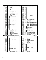
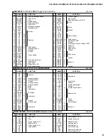
Page 1: ...D LAYOUT 7 BLOCK DIAGRAM 8 DISASSEMBLY PROCEDURE 9 LSI PIN DISCRIPTION 17 IC BLOCK DIAGRAM 22 CIRCUIT BOARDS 23 TEST PROGRAM 28 INSPECTION 31 MIDI IMPLEMENTATION CHART 32 PARTS LIST CIRCUIT DIAGRAM CLP 970 CLP 970C This document is printed on chlorine free ECF paper with soy ink Model equipped with A has no floppy disk drive CLP 970M ...

Page 2: ...efor inevitable and changes in specification are subject to change without notice or obligation to retrofit Should any discrepancy appear to exist please contact the distributor s Service Division WARNING Static discharges can destroy expensive components Discharge any static electricity your body may have accumulated by grounding yourself to the ground bus in the unit heavy gauge black wires conn...

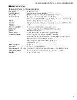
Page 3: ...le other Display LCD Recording playback 16 track recording playback tempo adjustment Disk drive 3 5 inch floppy disk drive 2DD and 2HD compatible Pedal Damper sostenuto soft Demo songs 6 voice demo songs 50 piano songs preset songs Jacks connectors AUX out R L L R Output impedance 600 ohm AUX in R L L R Input impedance 10 kohm Input sensitivity 0 26 V Headphone jacks x 2 TO HOST connector MIDI con...

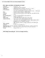
Page 4: ...le other Display LCD Recording playback 16 track recording playback tempo adjustment Pedal Damper sostenuto soft Demo songs 6 voice demo songs 50 piano songs preset songs Jacks connectors AUX out R L L R Output impedance 600 ohm AUX in R L L R Input impedance 10 kohm Input sensitivity 0 26V Headphone jacks x 2 TO HOST connector MIDI connectors IN OUT THRU pedal jack AUX PEDAL jack Main amplifiers ...

Page 5: ...O DOWN UP 14 A B NO YES C D 15 LCD screen 16 CONTRAST knob 17 EXIT 18 Voice group buttons for the MAIN section 19 SPLIT POINT 20 Voice group buttons for the LEFT section 21 VOICE SETTING Button 22 REVERB 23 CHORUS 24 BRILLIANCE Buttons 25 MIDI SETTING Button 26 OTHER SETTING 27 PHONES 28 Soft pedal 29 Sostenuto pedal 30 Damper pedal TOP Panel 1 2 3 4 5 6 7 8 9 10 11 12 13 15 16 17 18 19 20 21 22 2...

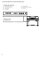
Page 6: ...P 970AC 32 33 34 35 36 37 38 31 31 AUX OUT R L L R 32 AUX IN R L L R 33 AUX PEDAL 34 TO HOST 35 HOST SELECT 36 MIDI IN OUT THRU 37 PEDAL 38 Floppy disk drive NOTE Model equipped with A has no floppy disk drive Terminal and Jack Panel Floppy disk drive ...

Page 7: ...Heat Sink And fix it by the Filament Tape so that a DM circuit board side may not become loose 80 81 Wire Hamess and Cable Holder B are not installed PARTS LIST REF NO CONNECTOR NAM PIN LENGTH DESTINATION Speaker Box Assembly 13 Panel Assembly 19 Panel Assembly 20 Panel Assembly 21 Main Unit 29 Main Unit 30 Main Unit 31 Main Unit 32 Main Unit 33 Main Unit 34 Main Unit 35 Main Unit 36 Main Unit 80 ...

Page 8: ...1MCLK IN OUT THRU MIDI DAMPER SOSTE SOFT PEDAL UNIT AUX PEDAL TRANS FOMER IC12 IC13 IC14 15 5 REG Phones To MA120 CN4 MELO MIXI RxD SYI TxD SYO To MA120 CN4 7 11 13 15 25 27 37 39 41 111 113 114 73 76 78 80 84 86 88 92 2 51 30 101 33 100 48 43 120 118 110 133 134 119 122 121 34 32 131 132 120 36 53 50 49 54 136 52 31 109 10 9 16 14 11 4 35 40 44 48 1 3 8 9 69 62 10 65 70 62 66 7 11 13 16 17 32 34 ...

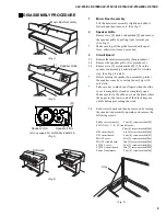
Page 9: ...g the ass y up with soft cloth Take care not to pinch your fingers when the slide cover is completely closed or completely open Make sure to fix the slide cover on the place where the upper or the lower end of the black keys are visible during proceeding the work 3 4 Each circuit board can then be removed by turning the speaker box assembly upwards and remove the following screws Shilde cover asse...

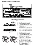
Page 10: ... The rack cover can then be removed See Fig 6 5 5 Set the left end of the rot at the slits of the guide and then lift the rear keycover assembly See Fig 8 5 6 Lean slightly the keycover assembly so that the rot can be removed from the guide rail See Fig 9 When removing be sure not to make scratches on the sideboard When reinstalling the keycover assembly apply a masking shield tape around the guid...

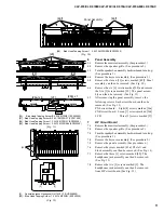
Page 11: ... marked 27 7 HP Circuit Board 7 1 Remove the music rest assembly See procedure 1 7 2 Remove the speaker grille See procedure 2 7 3 Turn the speaker box assembly backwards and turn it up See procedure 3 7 4 Remove the keycover assembly See procedure 5 7 5 Remove the panel assembly See procedure 6 7 6 Remove the screw marked 45a The left end block assembly can then be removed See Fig 14 7 7 Remove t...

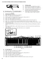
Page 12: ...crew marked 44 then the screw marked 42 10 PL Circuit Board 10 1 Remove the music rest assembly See procedure 1 10 2 Remove the speaker grille See procedure 2 10 3 Turn the speaker box assembly backwards and turn it up See procedure 3 10 4 Remove the keycover assembly See procedure 5 10 5 Remove the panel assembly See procedure 6 10 6 Remove the GH keyboard assembly See procedure 9 10 7 Remove the...

Page 13: ...ws marked 4b The 2 5cm speaker can then be removed See Fig 18 The left speaker and right speaker can be removed in the same manner 14 Main Unit 14 1 Remove the back board assembly See procedure 12 14 2 Disconnect the AC cord 14 3 Disconnect the PK cable 14 4 Remove the four 4 screws marked S3 Lift the main unit up slightly and then slide it to backward and then lift it up See Fig 19 Be sure to pla...

Page 14: ... the speaker box assembly See Fig 21 Take care not to draw away three 3 screws 48i Prior to remove the speaker box assembly disconnect the connector from the NW circuit board remove four 4 screws 48j to remove the cable assembly fastner See Fig 22 5 Bind Head Tapping Screw 1 3 5X16 MFZN2Y EP030190 7 Bind Head Tapping Screw 1 4 0X14 MFZN2Y EP040230 When reinstalling fit the notch of the hinge into ...

Page 15: ...ews marked 260A The AEXL88 H circuit board can then be removed See Fig 27 Keys can be removed without removing the circuit boards 18 C White Key Insert a thin plate between the white keys near the triangle mark around the fulcrum of the key and press down the stopper marked A to remove the key See Fig 28 and 29 Take care not to damage the key spring when removing a key A black key can be removed a...

Page 16: ...ing Place the GH keyboard assembly rightside up and fix a key spring to the frame by setting it at the slit and pushing it down once See Fig 33 Be careful of the direction of the spring 19 C White Black Key After a key has been fit to part F and the key guide make sure that the spring is fixed to the key Then press part E of the key down See Fig 34 19 D AEXL88 L circuit board Tighten the seven 7 s...

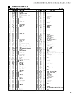
Page 17: ... strobe high 106 PLLVSS I PLL Ground 35 VSS I Ground 107 PA15 I O Port A 36 RDWR O DRAM read write 108 RES I Reset 37 A18 O 109 DREQ0 I DMA transfer request 38 A19 O Address bus 110 TIOC0B I O MTU input capture output compare ch 0 39 A20 O 111 PE2 I O Port E 40 VCC I Power supply 112 VCC I Power supply 41 A21 O Address bus 113 PE3 I O 42 VSS I Ground 114 PE4 I O Port E 43 RD O Read 115 PE5 I O 44 ...

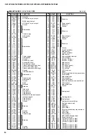
Page 18: ...U clock out 36 PB5 O DRAM read write 108 RES Reset 37 A18 O 109 TIOCOA I A D jack insert detect interrupt request input 38 A19 O Address bus 110 PE1 I Smart MINS 39 A20 O 111 PE2 I Model detection 40 VCC40 Power supply 112 VCC112 Power supply 41 A21 O Address bus 113 PE3 I Smart busy input 42 VSS42 Ground 114 PE4 I MLAN reset interrupt request input 43 RD O Read 115 PE5 O 1M clock cut 44 WDTOVF No...

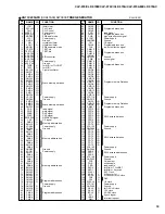
Page 19: ...7 SMD8 I O 121 CMD1 I O 38 SMD7 I O Wave memory data bus 122 CMD15 I O Program memory Data bus 39 SMD0 I O 123 CMD0 I O 40 SMD15 I O 124 CMA21 O Program address bus 41 SOE O read signal 125 PDT15 I O 42 SWE O write signal 126 PDT14 I O 43 SRAS O RAS signal 127 PDT13 I O 44 SCAS O CAS signal 128 PDT12 I O SWX access data bus 45 REFRESH O REFRESH signal 129 PDT11 I O 46 CS0 O CS signal 130 PDT10 I O...

Page 20: ...board 28 MD10 I O 68 KBSCLK O KBS clock 29 MD11 I O 69 XCLK1 I 30 MD12 I O 70 XCLK2 I KSN interface clock 31 MD13 I O 71 XCLK3 I 32 MD14 I O 72 KSEL I KBS KSN select 33 VDD Power supply 73 VDD Power supply 34 MD15 I O 74 ADSEL0 O 35 SCS I Slave CPU chip select 75 ADSEL1 O FSV interface CH select 36 SRD I Slave CPU read 76 ADSEL2 O 37 SWR I Slave CPU write 77 ADMCLK O FSV A D system clock 8 MHz 38 ...

Page 21: ...O 31 READY I Ready from FDD 63 MON3 O 32 WPRT I Write control signal 64 VSS9 Ground MBCG46183 129 XV833A00 GATE ARRAY DM IC004 PIN NAME I O FUNCTION PIN NAME I O FUNCTION NO NO 1 D5 I O 25 TX31 O 2 D6 I O Data bus 26 RX32 I 3 D7 I O 27 TX32 O Serial data 4 IRQ0 I O Interrupt request 28 RX33 I 5 IRQ1 I O Interrupt request 29 TX33 I O 6 VSS6 Ground 30 IC I Initial Clear 7 IRQ2 I O Interrupt request ...

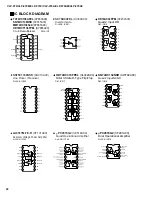
Page 22: ...er Gate 1 2 3 4 5 6 7 A B Select Enable Output B C C G2A G2A G2B G2B G1 G1 Y7 Y7 16 15 14 13 12 11 10 Vcc Y0 Y0 Y1 Y1 Y2 Y2 Y3 Output Y3 Y4 Y4 Y5 Y5 8 GND 9 Y6 TC74HC138AFEL XY863A00 SN74HC138NSR XY865A00 MM74HC138SJX XY867A00 HD74HCT138FPEL XY965A00 3 to 8 Demultiplexer A Y6 SWX IC5 D JACK IC001 DM IC019 DM IC017 D JACK IC002 DM IC018 µPC4570G2 XF291A00 Dual Operational Amplifier 1 2 3 4 V 8 7 6 ...

Page 23: ...N102 to SWX SLOT to A JACK CN210 to D JACK CN1 to D JACK CN2 to PNR CN202 not installed to GH Keyboard to MA120 CN4 Component side DM CIRCUIT BOARD 2NA V517300 Pattern side Note See parts list for details of circuit board component parts Note Model equipped with A has no floppy disk drive ...

Page 24: ...G START STOP DOWN UP SETTING METRONOME to DM CN9 to PNL CN103 to LCD NO YES EXIT PIANO SPLIT POINT E PIANO BASS PIANO E PIANO HARPSI CHORD HARPSI MALLET MALLET ORGAN STRINGS ORGAN BASS STRINGS CHOIR VOICE SETTING REVERB CHORUS BRILLIANCE MIDI SETTING OTHER SETTING PNL CIRCUIT BOARD PNR CIRCUIT BOARD Component side PNL 2NA V528910 PNR 2NA V528910 Component side Note See parts list for details of ci...

Page 25: ...R L L R R L L R to PNL CN101 to HP CN1 to DM CN3 to MA120 CN6 to DM CN10 16 A JACK CIRCUIT BOARD SWX CIRCUIT BOARD Component side Pattern side A JACK 2NA V493880 2 SWX 2NA V517320 2 Component side Pattern side Note See parts list for details of circuit board component parts ...

Page 26: ... CIRCUIT BOARD NETWORK CIRCUIT BOARD Component side Component side AUX PEDAL TO HOST HOST SELECT MIDI THRU OUT IN to PEDAL to DM CN4 to DM CN7 D JACK CIRCUIT BOARD Pattern side Component side to PK Cable Sostenute Pedal Soft Pedal PEDAL CIRCUIT BOARD Component side PEDAL VR CIRCUIT BOARD Damper Volume Component side D JACK 2NA V493830 1 PEDAL 2NA V233730 1 NETWORK 2NA V245500 1 HP 2NA V202110 PEDA...

Page 27: ... floppy disk drive to A JACK CN240 to NW CN1 to FU120 CN2 to FDD Power to DM CN2 not installed to MA120 CN1 to POWER SW V SELECTOR AC INLET to AEXL88L to AEXL88H to DM CN5 to HP CN2 POWER PL CIRCUIT BOARD FU120L CIRCUIT BOARD Component side Component side Component side Component side KSN2 CIRCUIT BOARD MA120 2NA VT14340 1 FU120L 2NA VV65070 1 KSN2 2NA V306660 PL 2NA VN63740 ...

Page 28: ...U Check the LED display s Main Ram Chk1 OK 7 007 Sub Ram Chk1 Check the Sub RAM Check all the RAMs on the buses of the Sub CPU Check the LED display s Sub Ram Chk1 OK 8 008 Flash Rom Chk1 Check the Flash ROM Check all the ROMs on the buses of the Main CPU Check the LED display s Flash Rom Chk1 OK 9 009 WaveRom Chk1 Check the Wave ROM Check all the ROMs on the buses of the CPU Check the LED display...

Page 29: ...ld be lower than R channel by more than 50 dB AUX OUT L 4 dBm PHONES L Should be lower than R channel by more than 40 dB PHONES R 7 dBm 24 024 EQ Low Checks EQ LOW frequency Checks if the output level of the sine wave 65 4 Hz C1 can be 15 dBm when the wave is output at PAN Center Measuring terminal MA120 CN5 or A JACK CN240 25 025 EQ Mid Checks EQ MID frequency Checks if the output level of the si...

Page 30: ...e pedal from MIN to MAX C3 is output when detecting that frequency is MIN and then C4 is output when the pedal functions normally 38 038 MIDI Chk After connecting the MIDI IN and MIDI OUT execute the test The test result appears on the LED display 39 039 To Host Chk Connect pin 1 to pin 2 pin 3 to pin 5 and pin 6 to pin 8 on the TO HOST terminal and execute the test Check that the following notes ...

Page 31: ...BASS A4 O 17 METRONOME SETTING B2 40 VOICE SETTING A 4 18 TEMPO DOWN C3 41 REVERB B4 O 19 TEMPO UP C 3 42 CHORUS C5 O 20 LCD A D3 43 BRILLIANCE C 5 21 LCD A D 3 44 BRILLIANCE D5 22 LCD C E3 45 MIDI SETTING D 5 23 LCD C F3 46 OTHER SETTING E5 1 AUX OUT and PHONES 1 1 Apply a 1 kHz 20 dBm sine wave to the AUX IN L L R Confirm that the output meets the following specifications AUX OUT L L R 9 dBm 2 d...

Page 32: ... v 1 127 X 8nH v 1 127 O v 1 127 O After Touch key s Ch s X X X O Pitch Bender X O 0 24 semi Control Change 0 32 1 5 7 10 11 6 38 64 66 67 65 71 74 84 91 93 94 96 97 98 99 100 101 120 121 O X X O O O X X X O X X O X X O X X O O O X X X O O X O O O Bank Select Modulation Portamento Time Data Entry Portamento Sound Controller Portamento Cntrl Effect Depth RPN Inc Dec NRPN LSB MSB RPN LSB MSB All sou...

Page 33: ... After Touch key s Ch s X X O 1 O 1 Pitch Bender X O 0 24 semi 1 Control Change 0 32 1 5 7 10 11 6 38 64 67 71 74 84 91 93 94 96 97 98 99 100 101 X X X X X X X X X X O 1 O 1 O 1 O 1 O 1 O 1 O 1 O 1 O 1 O 1 Bank Select Data Entry Sound Controller Portamento Cntrl Effect Depth RPN Inc Dec NRPN LSB MSB RPN LSB MSB Program Change True X O 0 127 System Exclusive X O System Common Song Position Song Sel...

Page 34: ...xport model 220V I Indonesian model N X General export model J Japanese model Y Export model WARNING Components having special characteristics are marked and must be replaced with parts having specifications equal to those originally installed KEYBOARD ASSEMBLY 16 PANEL ASSEMBLY 18 MA120 ASSEMBLY 20 FU120L ASSEMBLY 21 JACK UNIT 22 HEADPHONES JACK ASSEMBLY 23 FLOPPY DISK DRIVE ASSEMBLY 24 BENCH 25 ...

Page 35: ...2 CLP 970 CLP 970M CLP 970C CLP 970A CLP 970AM CLP 970AC S4 S2 23 5 24 13 S2 S1 S1 S3 1 22 21 OVERALL ASSEMBLY Front view Rear view S1 S2 S3 S4 S5 6 Screw set ...

Page 36: ...y フ ロ ッ ピ ー デ ィ ス ク 書 込 済 み F D 書 込 済 み F D 電 源 コ ネ ク タ 側 板 セ ッ ト L 側 板 セ ッ ト L 側 板 セ ッ ト L 側 板 セ ッ ト R 側 板 セ ッ ト R 側 板 セ ッ ト R ペ ダ ル B o x セ ッ ト ペ ダ ル B o x セ ッ ト ペ ダ ル B o x セ ッ ト 裏 板 セ ッ ト 裏 板 セ ッ ト 裏 板 セ ッ ト 付 属 品 同 梱 品 セ ッ ト 椅 子 同 梱 品 セ ッ ト 椅 子 同 梱 品 セ ッ ト 椅 子 フ ロ ッ ピ ー デ ィ ス ク 書 込 済 み F D 書 込 済 み F D ネ ジ セ ッ ト ネ ジ セ ッ ト バ イ ン ド 小 ネ ジ ト ラ ス 小 ネ ジ ト ラ ス 小 ネ ジ ト ラ ス 小 ネ ジ ト ラ ス T P 1 種 CLP 970 ...

Page 37: ...ping Screw 1 EN630230 1 G 40 Bind Head Tapping Screw 1 EP040230 2 H 47 Truss Head Tapping Screw 1 VU952600 2 J 38 Bind Head Tapping Screw 1 EP030240 2 K 46 Bind Head Tapping Screw B EP600190 8 N 43 Truss Head Screw VB934000 4 Q 45 Bind Head Tapping Screw 1 EP030470 4 S 52 Guide Screw VN887900 2 U 44 Bind Head Tapping Screw B EP600240 4 V 49 Bind Head Tapping Screw 1 EP030190 19 X 83 Bind Head Tapp...

Page 38: ...1600 V5827800 AAX16560 AAX18010 AAX17920 AAX18860 AAX18870 AAX18880 VN637600 VU659100 EP030340 V4961300 V4961400 V5828900 48 71 71 71 71 71 71 72 72 73 73 73 73 74 75 2 2 2 3 3 3 4 4 4 5 5 5 5 5 5 5a 5a 5b 5c 6 6 6 8 8 8 9 CLP 970M CLP 970AM V530910 CLP 970C CLP 970AC V559470 CLP 970 CLP 970A V499640 CLP 970M CLP 970AM V499650 CLP 970C CLP 970AC V582010 CLP 970 CLP 970A CLP 970 CLP 970A CLP 970M C...

Page 39: ...GHT 4 0X20 MFZN2BL 3 5X20 MFZN2BL 4 0X65 MFZN2Y TYPE M M6XL33 2 4 8 3 2 2 4 8 3 2 05 04 05 03 01 01 01 01 05 04 05 03 01 01 01 01 SIDE BOARD ASSEMBLY Side Board Assembly Side Board Assembly Side Board Assembly Side Board Side Board Side Board Stand Angle Bracket Angle Bracket Holder Back Board Stand Base Set Stand Base Set Stand Base Set Foot Flat Head Tapping Screw 1 Bind Head Tapping Screw 1 Pan...

Page 40: ... ド T P 1 種 ト ラ ス T P 1 種 CLP 970 CLP 970M CLP 970C CLP 970A CLP 970AM CLP 970AC CLP 970 CLP 970A V554850 CLP 970M CLP 970AM V554860 CLP 970C CLP 970AC V554870 CLP 970 CLP 970A CLP 970M CLP 970AM CLP 970C CLP 970AC 3 8 03 19 01 01 CL CL J CL CL J 115X12X2 RE H NK 3N 4 0X14 MFZN2Y 4 0X12 MFZN2BL PEDAL BOX ASSEMBLY Pedal Box Assembly Pedal Box Assembly Pedal Box Assembly Pedal Box Pedal Box Pedal Box...

Page 41: ...ER LEFT RIGHT PEDAL BL PEDAL PK LF 1 PEDAL PEDAL 3 0X8 MFZN2BL L 160 PEDAL PEDAL PEDAL PEDAL VOLUME BK 1 PEDAL ASSEMBLY Pedal Assembly Pedal Frame Pedal Piece Pedal Piece Pedal Piece Actuator Pedal Spring Felt Shutter Connector Assembly Rubber Contact Circuit Board Bind Head Tapping Screw B Adjuster Cord Binder Holder VR VR Holder Actuator VR Circuit Board Cord Holder V0053100 VU339700 VU362000 VU...

Page 42: ...70A V497520 CLP 970M CLP 970AM V582750 CLP 970C CLP 970AC V582760 CLP 970 CLP 970A V497810 CLP 970M CLP 970AM V582650 CLP 970C CLP 970AC V582660 V638300 3 2 3 20 2 05 01 01 CLAVINOVA 3 5X8 MFZN2 MUSIC REST ASSEMBLY Music Rest Assembly Music Rest Assembly Music Rest Assembly Music Rest Music Rest Music Rest Score Support Score Support Score Support Angle Bracket Plate Badge Foot Flat Head Tapping S...

Page 43: ...10 CLP 970 CLP 970M CLP 970C CLP 970A CLP 970AM CLP 970AC SPEAKER BOX ASSEMBLY Speaker Box Unit Speaker Grille Front view Front view Bottom view 1 19 18 6 7 10 11 12 3 2 1 1 4 2 8 9 16 16 17 4 2 5 6 9 1 ...

Page 44: ... 2 01 01 04 01 CL CL CL CL 16 cm 8 ohm 60W 2 5cm 8ohm 60W 4 0X16 MFZN2BL CL CL CL CL 3 5X25 MFZN2BL PK 6 2 0 2 MFZN2BL 2 0 2 MFZN2BL 3 5X16 MFZN2BL 480X6XT2 270X6XT2 BL 40 L 100 SP 1294X9X2T 280X15X0 55 SPEAKER BOX ASSEMBLY Speaker Box Assembly Speaker Box Assembly Speaker Box Assembly Speaker Box Unit Speaker Box Unit Speaker Box Unit Speaker Speaker Bind Head Tapping Screw 1 Speaker Box Unit Spe...

Page 45: ...12 CLP 970 CLP 970M CLP 970C CLP 970A CLP 970AM CLP 970AC SIDE COVER ASSEMBLY Side view 8 7 9 5 4 5 5 5 3 2 1 5 ...

Page 46: ... V520850 10 2 8 2 01 01 01 01 LEFT LEFT LEFT LEFT LEFT LEFT LEFT LEFT LEFT U 3 5X16 MFZN2Y 18 50 3 5X30 MFZN2BL RIGHT RIGHT RIGHT RIGHT RIGHT RIGHT RIGHT RIGHT RIGHT U 3 5X16 MFZN2Y 18 50 3 5X30 MFZN2BL SIDE COVER ASSEMBLY Side Cover Assembly Side Cover Assembly Side Cover Assembly Side Cover Side Cover Side Cover Guide Rail Guide Rail Rack Assembly Angle Bind Head Tapping Screw 1 Creat B Truss He...

Page 47: ...CLP 970A V528550 CLP 970C CLP 970AM V530910 CLP 970C CLP 970AC V559470 CLP 970 CLP 970A CLP 970M CLP 970AM CLP 970C CLP 970AC V522000 CLP 970 CLP 970M CLP 970A CLP 970AM CLP 970C CLP 970AC Power Power V580080 V533550 2 2 2 2 10 10 10 01 10 10 10 02 01 08 03 01 01 01 END BLOCK ASSEMBLY End Block Assembly End Block Assembly End Block Assembly End Block End Block End Block Angle Bind Head Tapping Scr...

Page 48: ...1 01 03 02 01 YMMA YCJ YMMA YCJ YMMA YCJ YCJ YCJ YCJ F R LEFT RIGHT 3 0X10 MFZN2Y 3 5X8 MFZN2BL 500 600X12 421X2 5X4 3 5X10 MFZN2Y KEY COVER ASSEMBLY Key Cover Assembly Key Cover Assembly Key Cover Assembly Key Cover Assembly Key Cover Assembly Key Cover Assembly Key Cover Key Cover Key Cover Key Cover Key Cover Sash F Assembly Guide Pin Sash Rod Gear Holder Rod Holder Rod Bushing Bind Head Screw ...

Page 49: ... CLP 970 CLP 970M CLP 970C CLP 970A CLP 970AM CLP 970AC KEYBOARD ASSEMBLY 90 10 20 110 30 60 70 80 280 200 340 210 220 250 240 260 260 230 120 160 130 170 140 180 150 190 310 300 350 270 110 40 50 110 100 ...

Page 50: ...ite Key White Key White Key White Key Black Key Hammer White Key Hammer White Key Hammer White Key Hammer White Key Hammer Black Key Hammer Black Key Hammer Black Key Hammer Black Key Stopper Stopper Rubber Contact Circuit Board Circuit Board Insulation Spacer Bind Head Tapping Screw P Spring Rubber Rubber 2 Connector Assembly Connector Assembly Protect Wire Stopper Support A Stopper Support A VU4...

Page 51: ...18 CLP 970 CLP 970M CLP 970C CLP 970A CLP 970AM CLP 970AC 1 33 2 32 3 3 34 3 3 3 4 16 17 18 24 25 25 25 25 30 23 22 31 PANEL ASSEMBLY Panel revers side Panel Fase side Panel revers side ...

Page 52: ...1 01 02 05 1 2 Z 1 2 3 4 5 6 7 8 9 10 11 PNL PNR 16P 350 15P 400 VOL L 400 12P 250 16P 125mm BK 1 3 0X8 MFZN2Y 2 6X10 MFZN2Y 3 5X10 MFZN2Y 3 5X12 MFZN2BL 12X50 MK BL PANEL ASSEMBLY Panel Assembly Panel Assembly Panel Assembly Panel Panel Panel Panel Front Angle Panel Holder Assembly Slide Knob Button Button Button Button Button Button Button Button Button Button Button LCD Circuit Board Circuit Bo...

Page 53: ...70AC J U B E N J U B E N 5 4 4 23 23 01 01 01 03 03 11 20 20 J U E GBR N 4 0X8 MFZN2Y 3 0X10 MFZN2Y 3 0X16 MFZN2Y MA120 J U MA120 E GBR N MA120 ASSEMBLY MA120 Assembly MA120 Assembly Bind Head Tapping Screw B Bind Head Tapping Screw B Bind Head Tapping Screw B Transistor Holder Transistor Holder Heat Sink Circuit Board Circuit Board VT492000 VT492100 EP640410 EP600220 EP600390 VT461100 VT461200 VT...

Page 54: ... B E VV65040 N VV65050 N N 4 2 2 13 13 12 01 07 07 12 01 01 J U E N 3 0X8 MFZN2BL FU120L FU120L FU120L FU120L 3 0X10 MFZN2BL 3 0 MFZN2Y FU120L ASSEMBLY FU120L Assembly FU120L Assembly FU120L Assembly FU120L Assembly Bind Head Tapping Screw B Panel AC Inlet Panel AC Inlet Circuit Board Circuit Board Circuit Board Circuit Board Bind Head Screw Hexagonal Nut VV651100 VV651300 VV651400 VV651500 EP6001...

Page 55: ... RANK RANK Japan only New Parts 1 4 2 3 4 4 JACK UNIT Front view Top view CLP 970 CLP 970M CLP 970C CLP 970A CLP 970AM CLP 970AC V582150 V582140 12 01 D JACK A JACK 3 0X8 MFZN2BL JACK UNIT Jack Unit Angle Jack Circuit Board Circuit Board Bind Head Tapping Screw B V5027200 V5276100 EP600190 1 2 3 4 ...

Page 56: ...P 970 CLP 970M CLP 970C CLP 970A CLP 970AM CLP 970AC VT15870 V004760 2 2 09 04 01 09 04 01 HP HP 12 0 14X2 MFZN2BL HP YI 12 0 14X2 MFZN2BL HEADPHONES JACK ASSEMBLY Headphones Jack Assembly Circuit Board Angle Headphone Hexagonal Nut Headphones Jack Assembly Circuit Board Angle Headphone Hexagonal Nut VT089300 VN631800 VB508600 VT089300 VN631800 VB508600 1 2 3 1 2 3 ...

Page 57: ...LY Note Model equipped with A has no floppy disc drive CLP 970 CLP 970M CLP 970C V499740 V590820 V523680 4 4 4 01 01 BL 1M 2M 359M3 3 0X5 MFZN2Y 1 2 3 0X8 8 MFZN2Y FLOPPY DISK DRIVE ASSEMBLY Floppy Disk Drive Assembly FDD Cover Floppy Disk Drive Bind Head Screw GND Wire 1 Bushing Holder FDD PW Head Tapping Screw B V4998200 V5667800 EG330150 VA121600 V2276900 1 2 3 5 7 8 9 ...

Page 58: ...70A U CLP 970M CLP 970AM U N CLP 970AC U 4 4 4 4 4 BC 100DR BC 100MH BC 100CH 1 10 0X1 25 MFZN2 2 10 0 MFZN2Y BENCH Bench Set Assembly Bench Set Assembly Bench Set Assembly Bench Board Assembly Bench Board Assembly Bench Board Assembly Wrench Leg Assembly Leg Assembly Leg Assembly Screw Set Hexagonal Nut Spring Washer V5532900 V5533000 V5533100 VT655900 V5533200 V5533300 V5533400 VS530500 03761250...

Page 59: ...WX XG AEXL88 L YMZ702 D PH 8P TE PH 9P TE PH 12P TE 1SS133 1SS176 0 01 50V Z 0 01 50V Z 100 00 10 0V 0 55 0 55 1 0M 1 4 J 100 0 1 4 J 100 0 1 4 J 1 0K 1 4 J CST4 00MGW040 RGLD12X103J AEXL88 H PH 9P TE PH 12P TE 1SS133 1SS176 A JACK 0 55 PH 8P TE PH 11P TE PH 7P TE XH 5P TE PH 9P TE XH 6P TE B 3900P 50V K B 1800P 50V K SL 180P 50V J SL 150P 50V J 4 7 25 0V 4 7 25 0V F 0 1 50V Z ELECTRICAL PARTS Cir...

Page 60: ...or Myler Capacitor Myler Capacitor Myler Capacitor Myler Capacitor Monolithic Ceramic Cap Monolithic Ceramic Cap Monolithic Ceramic Cap Electrolytic Cap BP Myler Capacitor Myler Capacitor Myler Capacitor Myler Capacitor Monolithic Myler Capacitor Monolithic Myler Capacitor Monolithic Myler Capacitor Monolithic Myler Capacitor Myler Capacitor Myler Capacitor Myler Capacitor Myler Capacitor Myler Ca...

Page 61: ...p Carbon Resistor chip Carbon Resistor chip Carbon Resistor chip Carbon Resistor chip Carbon Resistor chip Carbon Resistor chip Carbon Resistor chip Carbon Resistor chip Carbon Resistor chip Carbon Resistor chip Carbon Resistor chip Carbon Resistor chip Carbon Resistor chip Carbon Resistor chip Carbon Resistor chip Carbon Resistor chip Carbon Resistor chip Carbon Resistor chip Carbon Resistor chip...

Page 62: ...acitor CH Chip Ceramic Capacitor CH Chip Ceramic Capacitor B Chip Ceramic Capacitor B Chip Ceramic Capacitor F Chip Ceramic Capacitor F Chip Ceramic Capacitor B Chip Ceramic Capacitor B Chip Ceramic Capacitor B Chip Ceramic Capacitor B Chip Ceramic Capacitor B Chip Ceramic Capacitor B Chip Ceramic Capacitor F Chip Ceramic Capacitor F Chip Ceramic Capacitor SL Chip Ceramic Capacitor SL Chip Ceramic...

Page 63: ...3M J BK2125HS601 T BK2125HS601 T 56U LEM2520 T 560J 100 63M J 100 63M J 22K 63M J 100 63M J 100 63M J 3 9K 63M J 3 9K 63M J 10K 63M J 100 63M J 1 0M 63M J 1 0M 63M J 0 63M J 1 0K 63M J 1 0K 63M J 330 63M J 330 63M J 10K 63M J 0 63M J 2 2K 63M J 220 63M J 3 3K 63M J 1 5K 63M J 1 0K 63M J 1 0K 63M J 470K 63M J 470K 63M J 10K 63M J 10K 63M J IC IC IC IC IC IC IC IC IC IC IC IC IC IC IC IC IC IC IC IC...

Page 64: ...J 22K 63M J 22K 63M J 10K 63M J Carbon Resistor chip Carbon Resistor chip Carbon Resistor chip Carbon Resistor chip Carbon Resistor chip Carbon Resistor chip Carbon Resistor chip Carbon Resistor chip Carbon Resistor chip Carbon Resistor chip Carbon Resistor chip Carbon Resistor chip Carbon Resistor chip Carbon Resistor chip Carbon Resistor chip Transistor Array Transistor Transistor Digital Transi...

Page 65: ... Board AC Inlet Fuse Holder Jumper Wire AC Inlet Voltage Selector Fuse Holder Capacitor Capacitor Capacitor Base Post Connector Base Post Connector Fuse Fuse Fuse Fuse Jumper Wire Coil Jumper Wire Coil Coil Circuit Board Semiconductive Cera Cap Coil Carbon Resistor Phone Jack Connector Base Post Connector Base Post Jumper Wire Earth Wire Circuit Board Circuit Board Support PCB Support PCB Fuse Hol...

Page 66: ...nnector Base Post Connector Connector Base Post Base Post Connector Connector Base Post Diode Diode Diode Stack Diode Stack Diode Stack Fuse Fuse Fuse Fuse Fuse Fuse IC IC IC IC IC Fuse Resistor Fuse Resistor Carbon Resistor Carbon Resistor Carbon Resistor Carbon Resistor Carbon Resistor Fuse Resistor Fuse Resistor Carbon Resistor Carbon Resistor Carbon Resistor Carbon Resistor Metal Oxide Film Re...

Page 67: ...S133 1SS176 GL3ED8 GL3ED8 GL3ED8 SLZ 181B 09 T6 RE SLZ 181B 09 T6 RE SLZ 181B 09 T6 RE SLZ 181B 09 T6 RE SLZ 181B 09 T6 RE SLZ 181B 09 T6 RE SLZ 181B 09 T6 RE SLZ 181B 09 T6 RE SLZ 181B 09 T6 RE SLZ 181B 09 T6 RE SLZ 181B 09 T6 RE SLZ 181B 09 T6 RE SLZ 181B 09 T6 RE SLZ 181B 09 T6 RE SLZ 181B 09 T6 RE 82 0 1 4 J 82 0 1 4 J 82 0 1 4 J 82 0 1 4 J 0 55 56 0 1 4 J 56 0 1 4 J Transistor Transistor Tran...

Page 68: ... SKHVBL042A H 7 SKHVBL042A H 7 SKHVBL042A H 7 SKHVBL042A H 7 SKHVBL042A H 7 SKHVBL042A H 7 SKHVBL042A H 7 SKHVBL042A H 7 SKHVBL042A H 7 SKHVBL042A H 7 SKHVBL042A H 7 SKHVBL042A H 7 SKHVBL042A H 7 SKHVBL042A H 7 SKHVBL042A H 7 SKHVBL042A H 7 SKHVBL042A H 7 2SA1708 S T 2SC1740S R S 2SC1740S R S 1B10K RS30112A9A02 B10 0K RK09K1130BN MTZJ10B 10 0V SWX A 20P 53319 0200 22 6 3V 22 6 3V 0 01 50V K 0 01 5...

Page 69: ...Header Electrolytic Cap chip Electrolytic Cap chip Ceramic Capacitor B Chip Ceramic Capacitor B Chip IC IC IC IC IC IC IC IC Socket Carbon Resistor chip Carbon Resistor chip Carbon Resistor chip Carbon Resistor chip Carbon Resistor chip Carbon Resistor chip Circuit Board Connector Header Electrolytic Cap chip Electrolytic Cap chip Ceramic Capacitor B Chip Ceramic Capacitor B Chip IC IC IC IC IC IC...

Page 70: ...rolytic Cap chip Ceramic Capacitor B Chip Ceramic Capacitor B Chip IC IC IC IC IC IC Socket Carbon Resistor chip Carbon Resistor chip Carbon Resistor chip Carbon Resistor chip Carbon Resistor chip Carbon Resistor chip Carbon Resistor chip AC Cord Set AC Cord Set AC Cord Set AC Cord Set AC Cord Set AC Cord Set AC Cord Set AC Cord Set AC Cord Set Connector Power Transformer Power Transformer Power T...

Page 71: ...E ROM 2 WAVE ROM 3 WAVE ROM 4 DRAM 4M SRAM 256K SRAM 256K PROGRAM RAM DECODER A JACK OP AMP OP AMP OP AMP EQUALIZER OP AMP D JACK PHOTO COUPLER LINE FILTER INVERTER NJM79M12FA XD343A00 REGULATOR 12V 1 2 3 1 OUTPUT 2 INPUT 3 COMMON 1 OUTPUT 2 COMMON 3 INPUT 3 2 1 MJM78L05UA XJ598A00 REGULATOR 5V NJM78M12FA XJ602A00 REGULATOR 12V 1 OUTPUT 2 COMMON 3 INPUT 1 2 3 1 COMMON 2 INPUT 3 OUTPUT NJM79L05UA X...

Page 72: ...8H AEXL 88L WIRE TRAP 12P CABLE HOLDER 12P PH TE 14P PH TE 16P Power indicator Keybed PHONES HP PL MA120 FU120L NETWORK DESTINATION MODEL NON POLARIZED NON POLARIZED NON POLARIZED POLARIZED Not installed Not installed Installed Not installed 0 01uF 250V 0 01uF 250V 0 01uF 250V 0 01uF 250V 0 0047 250V 0 0047 250V 0 0047 250V 0 0047 250V Installed Installed Not installed Installed Not installed Not ...

Reviews: