VL-1000 Technical Supplement
Alignment
Forward ALC Adjustment (High Power)
Ì
Tune the transceiver to 14.050 MHz, FM mode,
and set the
DRIVE
or
RF PWR
control fully
clockwise.
Ì
Press and hold in the
INPUT
switch on the front
panel of the VL-1000 for ½ second. This initiates
the “ALC Alignment” mode.
Ì
Start with the transceiver’s
DRIVE
or
RF PWR
control fully counter-clockwise, then rotate the
DRIVE
or
RF PWR
control to the fully clock-
wise position while transmitting.
Ì
If the power output from the amplifier (as dis-
played on the
AVG PWR
meter) does not reach
1000 W because of the effect of the VL-1000’s ALC
voltage at full excited drive, keep the transceiv-
er’s
DRIVE
or
RF PWR
control fully clockwise,
then press and hold in the
DISPLAY 2
key until
the power output from the amplifier reaches 1000
Watts.
Ì
If, on the other hand, the ALC voltage from the
VL-1000 does not cause the exciter drive to be
controlled such that the power output from the
amplifier limits at 1000 Watts, reduce the setting
of the
DRIVE
or
RF PWR
control to that the out-
put power is 1000 Watts. Now press and hold in
the
DISPLAY 2
key until you observe the ampli-
fier output
just begin
to fall below 1000 Watts. At
this point, advance the
DRIVE
or
RF PWR
con-
trol fully clockwise, and press/hold in the
DIS-
PLAY 1
or
DISPLAY 2
key so as to achieve 1000
Watts of power output.
Ì
If the above adjustments are not successful, it is
possible that the Forward ALC potentiometer,
VR1001, is maladjusted. While transmitting,
slowly rotate VR1001 in the direction that pro-
vides improved output control (either more or
less ALC voltage, as observed on the transceiv-
er’s ALC meter). When 1000 Watts of output
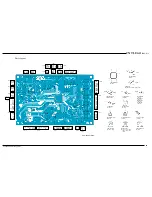
VR5004: Idling Current (800 mA)
VR5003: Idling Current (610 mA)
VR5002: Idling Current (800 mA)
VR5001: Idling Current (610 mA)
J5001: Remove this wire when adjusting the other PA Unit
J5007: Remove this wire when adjusting the other PA Unit
PA Unit Alignment Points
Summary of Contents for VL-1000
Page 8: ...VL 1000 Technical Supplement Chip Component Information Notes...
Page 11: ......
Page 12: ......
Page 13: ......
Page 14: ......
Page 20: ...VL 1000 Technical Supplement Alignment Notes...
Page 21: ...VL 1000 Technical Supplement Block Diagram...
Page 22: ...VL 1000 Technical Supplement Interconnection Diagram...
Page 24: ...VL 1000 Technical Supplement CNTL Unit Notes...
Page 26: ...VL 1000 Technical Supplement CNTL Unit Chip Side...
Page 27: ...VL 1000 Technical Supplement CNTL Unit Lot 2 Circuit Diagram...
Page 28: ...VL 1000 Technical Supplement CNTL Unit Lot 2 Notes...
Page 30: ...VL 1000 Technical Supplement CNTL Unit Lot 2 Chip Side...
Page 37: ...VL 1000 Technical Supplement Tuner Unit Circuit Diagram...
Page 38: ...VL 1000 Technical Supplement Tuner Unit Notes...
Page 40: ...VL 1000 Technical Supplement Tuner Unit Chip Side...
Page 41: ...VL 1000 Technical Supplement Circuit Diagram Tuner Unit Lot 4...
Page 42: ...VL 1000 Technical Supplement Notes Tuner Unit Lot 4...
Page 44: ...VL 1000 Technical Supplement Chip Side Tuner Unit Lot 4...
Page 46: ...VL 1000 Technical Supplement Chip Side Tuner Unit Lot 7...
Page 50: ...VL 1000 Technical Supplement Tuner Unit Notes...
Page 51: ...VL 1000 Technical Supplement LPF Unit Circuit Diagram...
Page 52: ...VL 1000 Technical Supplement LPF Unit Notes...
Page 54: ...VL 1000 Technical Supplement LPF Unit Solder Side...
Page 55: ...VL 1000 Technical Supplement LPF Unit Lot 4 Circuit Diagram...
Page 56: ...VL 1000 Technical Supplement LPF Unit Lot 4 Notes...
Page 58: ...VL 1000 Technical Supplement LPF Unit Lot 4 Solder Side...
Page 63: ...VL 1000 Technical Supplement Divider Unit Circuit Diagram...
Page 64: ...VL 1000 Technical Supplement Divider Unit Notes...
Page 66: ...VL 1000 Technical Supplement Divider Unit Solder Side...
Page 67: ...VL 1000 Technical Supplement Circuit Diagram Divider Unit Lot 3...
Page 68: ...VL 1000 Technical Supplement Divider Unit Lot 3 Notes...
Page 70: ...VL 1000 Technical Supplement Solder Side Divider Unit Lot 3...
Page 74: ...VL 1000 Technical Supplement PA Unit Notes...
Page 76: ...VL 1000 Technical Supplement PA Unit Solder Side...
Page 77: ...VL 1000 Technical Supplement PA Unit Lot 5 Circuit Diagram...
Page 78: ...VL 1000 Technical Supplement PA Unit Lot 5 Notes...
Page 80: ...VL 1000 Technical Supplement PA Unit Lot 5 Solder Side...
Page 84: ...VL 1000 Technical Supplement PA Unit Notes...
Page 85: ...VL 1000 Technical Supplement Display Unit Circuit Diagram...
Page 86: ...VL 1000 Technical Supplement Display Unit Notes...
Page 92: ...VL 1000 Technical Supplement Display Unit Notes...
Page 93: ...VL 1000 Technical Supplement ANT SW Unit Circuit Diagram...
Page 94: ...VL 1000 Technical Supplement ANT SW Unit Notes...
Page 99: ...VL 1000 Technical Supplement Line Filter Unit Circuit Diagram...
Page 100: ...VL 1000 Technical Supplement Line Filter Unit Notes...
Page 102: ...VL 1000 Technical Supplement Line Filter Unit Notes...
Page 110: ...VL 1000 Technical Supplement Relay Unit Notes...
Page 112: ...VL 1000 Technical Supplement Filter Unit AC Power Supply VP 1000 Notes...
Page 114: ...VL 1000 Technical Supplement Filter Unit AC Power Supply VP 1000 Notes...
Page 115: ......
Page 116: ......
Page 117: ......
Page 118: ......
Page 119: ......
Page 120: ......
Page 121: ......
Page 122: ......
Page 123: ......
Page 124: ......
Page 125: ......
Page 126: ......
Page 127: ......
Page 128: ......
Page 129: ......
Page 130: ......
Page 131: ......


