background image

NO.

Name

NO.

Name

21

connector cover

20

speaker box connector

19

speaker  box front cabinet

18

speaker grille

17

acryl  panel

16

speaker

37

rear cabinet cover(lower)

15

light indicator

36

rotate axis cover(back)

14

speaker box rear cabinet

35

rotate axis assy'

13

main board supporter assy'

34

column

12

metallic terminal panel(left)

33

stand upper cover

11

plastic terminal panel(left)

32

stand lower cover

10

PCMCIA card slot

31

rubber cushion

9

PCMCIA board

30

rear cabinet

8

PCMCIA card door

29

speaker box socket

7

PCMCIA bracket

28

shielding cover

6

button

27

main board

5

BUTTON panel

26

metallic terminal panel(right)

4

KEY supporter

25

plastic terminal panel(right)

3

rotate axis cover(back)

24

LCD panel

2

rear cabinet cover(upper)

23

remote sensor

1

rear cabinet cover

22

connector assy'

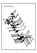
Exploded views list

22

Summary of Contents for LC22K9

Page 1: ...COLOR TELEVISION LC22K9 ...

Page 2: ...ting Trouble shooting Principle analysis of LC 22K9 LC22K9 BLOCK DIAGRAM 0 Wiring diagram Components No Identification criteria for the bright spot and dark spot of the LCD screen Troubleshooting guide Exploded views Schematic diagram 1 3 6 9 10 15 16 17 18 21 23 ...

Page 3: ...or damage to the set 2 4 Never operate the set or do any installation work in bad environment such as wet bathroom laundry kitchen or nearby fire source heating equipment and devices or exposure to sunlight etc Otherwise bad effect will result 2 5 If any foreign substance such as water liquid metal slices or other matters happens to fall into the module be sure to cut the power off immediately and...

Page 4: ...re tabulated as follows Temperature Scope for operation 0 50 C Scope for storage 20 60 C humidity Scope for operation 20 85 Scope for storage 10 90 2 13 Display of a fixed picture for a long time may result in appearance of picture residue on the screen as commmonly called ghost shadow The extent of the residual picture varies with the maker of LCD screen This phenonmenon doesn t represent failure...

Page 5: ...gree brightness about 9nit by R G B CUT to set the color coordinates of second gray degree to 270 283 Adjust R G B DRV to set the color coordinate of seventh gray degree to 270 and 283 Note Because the values of R G B CUT and R G B DRV directly determines the values of brightness and contrast at the DVI terminal of monitor board the white balance should be adjusted according to the preset value st...

Page 6: ...f the display is normal Method to enter factory menu Continuously push key of VOL Mute Video to enter factory menu When the first line of each and every adjusting item is in the highest brightness push Check if FLASH is written Production of the main board and decoders on the line Check Monitor board Check decoders in media board General assembly and combined calibration Connect central signal sou...

Page 7: ...in_G gain_B again and again until two gray degrees are 313 and 293 Selct mode to be 9300K adjust offset_R offset_G offset_B to set second color coordinate to 281 311 and the brightness to about 5nit Fix gain_G as 128 adjust gain_R gain_B to set seventh color coordinate to 281 311 Adjust offset_R offset_G offset_and gain_R gain_B again and again until two gray degrees are 281 313 Select mode to be ...

Page 8: ...push the auto adjust key on the remote control set once more check if the display is normal 3 4 Inspection of PCMCIA channel Insert PCMCIA card switchover to this channel and check if the display is normal 3 5 Inspecting sound channel Inspect if the output of speaker and earphone of channels is normal Trouble shooting Before servicing please check to find the possible causes of the troubles accord...

Page 9: ...he liquid crystal TV set and make proper adjustment according to the signal types Picture too bright and there is distortion in the brightest area Check if the contrast setting is too high Possibly the output quality of DVD broadcaster is set too high It maybe also due to improper terminal connection of the video frequency signal in a certain position of the system Picture is whitish or too bright...

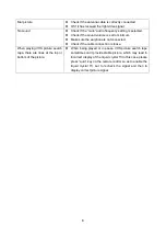
Page 10: ...nected Check if the cable connection is loose When playing VHS picture search tape there are lines at the top or bottom of the picture When being played or in pause VHS picture search tape sometimes can t provide stable picture which may lead to incorrect display of the liquid crystal TVIn this case please press auto key on the remote control so as to enable the liquid crystal TV set to recheck th...

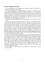
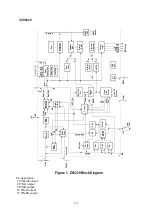
Page 11: ... subject to selection for conversion together with other two routes and then processed for digital display including OSD AND GAMMA correction and brightness and contrast processing and changed into 1024 768 format The RGB signal with 24BIT is output to the LVDS converter U31 DS90C383A for conversion into the signal format which the screen can accept that is three pairs of low voltage differential ...

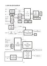
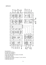
Page 12: ...T U32 CCD V CHIP Z86229 FB V U30 ADC MST9883 YPrPb U3 EEPROM U2 MICRO CONTRLER TSC80251G2D U4 FLASHMEMORY IR SIF AV1 SVHS R L AV2 R L YPrPb R L DVI R L VGA R L PCMCI R L AV R L OUT N201 AUDIO PROCESSOR MSP3420 U34 HEF4052 N203 SRS 3D STEREO CONTROLLER M62494 N205 N208 N210 D CLASS AUDIO AMPLIFIER LX1722 Si4532DY N212 TLE2142 HEADPHONE R L SPEAKER LC22K9 BLOCK DIAGRAM 10 RGB I C BUS 2 24bit YUV KEY...

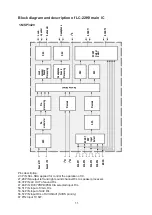
Page 13: ... Prescale 2 I S1 2 I S2 Sound IF1 Sound IF2 speaker 1 MSP3420 11 Block diagram and description of LC 22K9 main IC Pins description 2 3 PIN SCL SDA applied for control the operation of IC 27 28 PINAoutput left and right sound channel R L to speaker processor 36 37 PIN AV OUT of sound R L 47 48 PIN DVI YPRPB PCMCIA selected input R L 50 51 PIN Input of VGA R L 53 54 PIN Input of AV2 R L 56 57 PIN In...

Page 14: ...RGB FB Y Cr Cb Y Cr Cb Y G U B Y Cr Cb LL Clock Saturation Tint Analog Front end Contrast Brightness Peaking Clock Gen 2 I C Bus V R FB FB YCrCb RGB YCrCb 2 ADC Analog Component Front End 4 x ADC Processing 2 VPC3230 12 Pins description 4 PIN Input U of PCMCIA 5 73 PIN Input Y of PCMCIA 6 PIN Input V of PCMCIA 31 34 37 40 PIN output format signal of ITU R656 70 PIN Video of AV OUT 71 PIN Input C o...

Page 15: ... LPF Loop 1 Filter DOT CLK DIV Line CHAR CIR V Lock Field FLD LS SFLD SLS Control CHAR CLK CW Line Fld Decodes MSGR DOT CLK SMS SEN SCK SDA SDO 6 4 15 14 16 13 VDD 5V 12 11 2 I C SEL Vss A RREF POR CKT 4 10 Command Processor Row Address MUX Display RAM Character Generator Row Latch Display Latch SS CTR Output Logic 10 6 8 13 4 FLD V I Ref RED GREEN BLUE BOX 17 3 2 18 Addr Bus ADDR DEC 8 ADDR Decod...

Page 16: ... SLOT 0 PIP OVRLY SYNC BE FIFO 48 VID PIX DROP VGA VIDEO MUX SCALE SLOT 1 SCALE SLOT 2 MEM BE FIFO SCALE 48 24 24 16 24 48 CLUT GAMMA OSD OVERLAY DITHER ENGINE DATA STEER SDRAM INTERFACE MEM CAP FIFO MEM PACKER 48 128 128 UNPACKER MEM 128 128 48 OSD PANEL CTRL Panel clk Vga half clk Video half clk PANEL SDRAM 48 64 48 32 Scaling clk Memory clk SMARTSET SURE SYNC VID FIFO VGA FIFO FIFO MEM DIS FE 4...

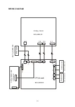
Page 17: ...7 L22K9 09 X212 X204 X201 X213 P2 PCMCIA card 667 L22K9 05 667 L40D9 90 P40 P41 P6 P8 P32 VIDEO P37 AUDIO P11 CONTROL P4 PANEL INTERFACE P39 IR POWER P29 BACKLIGHT 15 WIRING DIAGRAM LCD panel Keyboard CPU board Analog board 667 L22K9 53 667 L22K9 56 ...

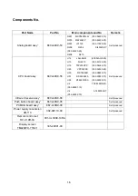
Page 18: ... 23100 00 U15 TFP403PZP 353 04030 10 U29 VPC3230D 353 32300 80 U30 MST9883B 353 98830 10 U31 DS90C383A 353 03830 70 U32 Z8622912SS 353 86229 10 U2 TSC80251G2D 353 80251 10 U4 AT49F002NT 352 49002 70 Self produced Infra red receive assy 667 L22K9 09 Self produced Push button board assy 667 L22K9 05 Self produced PCMCIA board assy 667 L40D9 90 Self produced Power supply conversion AD 11C 302 AD11C 0...

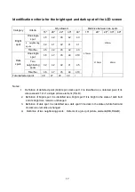
Page 19: ...0mm 5mm Total defected point 8 7 5 4 Notes 1 Definition of defected point bright spot dark spot It is identified as a defected point if its area exceeds 1 2 of a single picture element R G B 2 Definition of bright spot It is identified as a bright spot if it is bright in the state of dark field and its bright size remains unchanged 3 Definition of dark spot It is identified as a dark spot if it is...

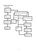
Page 20: ...fuse of power adapter is blown out Chang the power adapter Push key on the R C set or push power key to put on the set to check the status of the indication lamp Check F1 F2 if they are blown out Change CPU board Push any key on R C set to see if the indication lamp twinkles Check 12th foot of P29 is at high voltage Check 19th and 20th foot of P4 are at high electric level Check if F3 is blown out...

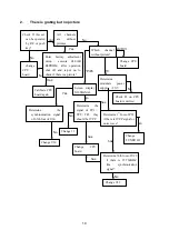
Page 21: ... picture change CPU board Calibrate CPU board again Change CPU board Screen display NO SIGNAL Determine modulate power supply 5V V Determine the synchronization signal of 65th foot of U30 Change U30 Check FI on CPU board is melted Determine 1st foot of P32 if there is 1VPP signal or noise wave Change TUNER 201 Determine 56th foot of U29 if there is 15 734KHZ line synchronization signal Change U29 ...

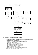
Page 22: ...tical or horizontal line interfere Screen no good 7 Sound no good line of FB20 P6 or speaker no good 8 Earphone no good C275 copper foil broken 9 Remote control no good X2 joint soldering line of R2 X2 no good 10 Function of push key abnormal line of X1 no good Check if R282 burns Check if TP2 is tri angle wave Change N207 Check the output wave form of foot 5 and 8 of N203 Check the output wave fo...

Page 23: ...EXPLODED VIEWS 21 ...

Page 24: ...ic terminal panel left 33 stand upper cover 11 plastic terminal panel left 32 stand lower cover 10 PCMCIA card slot 31 rubber cushion 9 PCMCIA board 30 rear cabinet 8 PCMCIA card door 29 speaker box socket 7 PCMCIA bracket 28 shielding cover 6 button 27 main board 5 BUTTON panel 26 metallic terminal panel right 4 KEY supporter 25 plastic terminal panel right 3 rotate axis cover back 24 LCD panel 2...

Page 25: ......

Page 26: ......

Page 27: ......

Page 28: ......

Page 29: ......

Page 30: ......

Page 31: ......

Page 32: ......

Page 33: ......

Page 34: ......

Page 35: ......

Page 36: ......

Page 37: ......

Page 38: ......

Page 39: ......

Page 40: ......

Page 41: ......

Page 42: ......

Page 43: ......

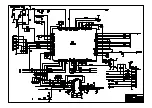
Page 44: ...CB55 0 1UF CB17 0 1UF CB37 0 1UF R24 0 OHM 1 2 CB23 100UF CB40 0 1UF IN 3 OUT 2 ADJ 1 N13 2830 3 3V CB36 0 1UF CB4 0 1UF CB5 0 1UF 1 2 CB22 10UF 1 2 X2 Power 1 2 CB34 10UF CB29 0 1UF CB9 0 1UF 1 2 CB10 10UF VCC33E VCCL VCC VCC33P VCC33 VCC VCC33 VCC VCCA VCC33 VCCA VCC 3 3V REGUALTOR EZ1085 No need to installEZ1085 circuitry if J12 provide 3 3V ES60x8 ADJ 24C01 OUT SDRAM WM8706 INP FRONT place nea...

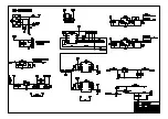
Page 45: ... 14 D6 17 D7 18 OC 1 CLK 11 Q0 2 Q1 5 Q2 6 Q3 9 Q4 12 Q5 15 Q6 16 Q7 19 N2 74HCT374 V1 FDN338P 1 2 C5 100UF 1 2 C7 47UF C8 0 1UF C14 0 1UF C12 0 1UF R11 10K V2 FDN338P R12 10K GND1 1 D3 2 D4 3 D5 4 D6 5 D7 6 CE1 7 A10 8 OE 9 A11 10 A9 11 A8 12 A13 13 A14 14 WE PGM 15 IREQ 16 VCC1 17 VPP1 18 A16 19 A15 20 A12 21 A7 22 A6 23 A5 24 A4 25 A3 26 A2 27 A1 28 A0 29 D0 30 D1 31 D2 32 IOIS16 33 GND 34 GND3...

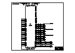
Page 46: ... LD0 RST LA5 LA16 LA17 LA11 LA10 LD3 LD1 LA13 LA15 LA3 LA8 LA0 LA21 LA19 LA6 LD4 LA12 LA7 LA1 LD2 LA14 LD 0 7 LA 0 19 LD 0 7 A0 12 A1 11 A2 10 A3 9 A4 8 A5 7 A6 6 A7 5 A8 27 A9 26 A10 23 A11 25 A12 4 A13 28 A14 29 A15 3 D0 13 D1 14 D2 15 D3 17 D4 18 D5 19 D6 20 D7 21 A16 2 CE 22 OE 24 A18 31 A17 30 A19 1 VCC 32 GND 16 N9 OPEN 27C040 080 90 VCC LD 0 7 4 PIN EXTENSION FOR ROM EMULATOR INTERFACE 4MBI...

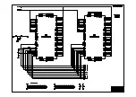
Page 47: ... 66 VSS 67 DCAS 69 DSCK DOE 70 DWE 71 DRAS0 72 DBANK0 DRAS1 73 DBANK1 DRAS2 74 VSS 76 DB0 77 DB1 78 DB2 79 DB3 80 DB4 81 DB5 82 VSS 84 DB6 85 DB7 86 DB8 87 DB9 88 DB10 89 DB11 90 VSS 91 DB12 93 DB13 94 DB14 95 DB15 96 DCS1 97 VSS 98 DQM 101 DSCK 102 VSS 103 CLK 105 AVSS VDAC 112 PCLK2XSCN CAMYUV4 116 PCLKQSCN CAMYUV5 AUX3 2 117 VSSCN CAMYUV6 EAUX3 1 118 HSSCN CAMYUV7 EAUX3 0 119 VSS 120 VSS 138 HW...

Reviews: