background image

Zynq-7000 AP SoC and 7 Series FPGAs MIS v4.1

86

UG586 November 30, 2016

www.xilinx.com

Chapter 1:

DDR3 and DDR2 SDRAM Memory Interface Solution

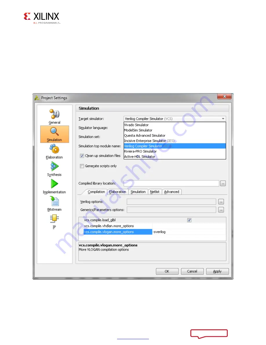
a. Browse to the 

Compiled libraries location

 and set the path on 

Compiles libraries 

location

 option.

b. Under the 

Compilation

 tab, set the 

vcs.compile.vlogan.more_options

 to 

-sverilog

.

c. Under the 

Simulation

 tab, set the 

vcs.simulate.runtime

 to 1 ms (there are 

simulation RTL directives which stop the simulation after a certain period of time 

which is less than 1 ms) as shown in 

Figure 1-49

.

3. Apply the settings and select 

OK

.

4. In the 

Flow Navigator

 window, select 

Run Simulation

 and select 

Run Behavioral 

Simulation

 as shown in 

Figure 1-47

.

X-Ref Target - Figure 1-49

Figure 1-49:

Simulation with VCS

Send Feedback

Summary of Contents for Zynq-7000

Page 1: ...Zynq 7000 AP SoC and 7 Series Devices Memory Interface Solutions v4 1 User Guide UG586 November 30 2016...

Page 2: ...nk Machines bullet in the Controller Options section 06 08 2016 4 0 DDR3 and DDR2 Updated Memory Part description in Controller Option section Added app_ecc_single_err 7 0 in Table 1 17 User Interface...

Page 3: ...pdated Read Stage 1 Debug Signal Map table Updated Calibration of Read Clock and Data description 09 30 2015 2 4 Added CLOCK_DEDICATED_ROUTE Constraints in all sections DDR3 and DDR2 Updated Trace Len...

Page 4: ...on Stages Updated description in Determine the Failing Calibration Stage section Updated Table 1 100 DDR2 DDR3 Debug Signals Updated Table 1 102 Debug Signals of Interest for Write Leveling Calibratio...

Page 5: ...description in FPGA Option section Updated C_S_AXI_DATA_WIDTH description in Table 1 19 AXI4 Slave Interface Parameters Updated Fig 1 50 Clocking Architecture Updated OCLKDELAYED Calibration section U...

Page 6: ...als of Interest for PRBS Read Leveling Calibration Chapter 2 Added reference to data sheet in Introduction section Updated package length descriptions in Trace Length Requirements section Added CPT_CL...

Page 7: ...Added CK description in Trace Lengths section Added new code constraints for DDR3 DDR2 Configuration sections Added Clocking section Updated ocal signals in Table 1 102 DDR2 DDR3 Debug Signals Chapter...

Page 8: ...component name user_design section Added OOC description in Customizing the Core section Added simulator flows Added ILA trigger settings in Vivado Lab Tools section Chapter 3 Added Out of Context con...

Page 9: ...ebug Signals of Interest for OCLKDELAYED Calibration Chapter 2 Updated Table 2 3 sim do description and simulation directory Updated DIFF_HSTL_I in I O Standards table Updated reference clock descript...

Page 10: ...ols section Added AR 54025 for Vivado Updated Debugging PHASER_IN DQSFOUND Calibration Failures dbg_pi_dqsfound_err 1 section Chapter 2 Updated ChipScope to Vivado logic analyzer VIO and ILA Added Fix...

Page 11: ...mination description in LPDDR2 Pinout Examples section Chapter 6 Added Upgrading the ISE CORE Generator MIG Core in Vivado section 03 20 2013 1 9 ISE 14 5 and Vivado Design Suite 2013 1 releases for M...

Page 12: ...ters Added description in Verifying the Simulation Using the Example Design section Chapter 3 Added No Buffer option description in FPGA Options section Updated Fig 3 14 FPGA Options Added Verify Pin...

Page 13: ...description in Bank and Pin Selection Guides for DDR2 Designs Added DDR2 SDRAM interface description to Configuration Chapter 2 Updated Table 2 2 and 2 7 to 2 8 with new table note and v name Added de...

Page 14: ...ion Chapter 4 Added System Clock Sharing section Chapter 5 Updated figures 5 15 5 17 to 5 20 updated steps in Getting Started with Vivado MIG IP Generation 07 25 2012 1 6 MIG 1 6 release Updated ISE D...

Page 15: ...d SSTL15 to HSTL_I Revised I O standards for sys_rst option in System Pins Selection Revised the PHY_BITLANE parameters in Table 2 11 Added System Clock PLL Location and Constraints and Configuration...

Page 16: ...ed tZQI and added USER_REFRESH Added Table 1 94 In Configuration updated constraints example and removed paragraph about SCL and SDA Chapter 2 Added step 2 to MIG Output Options page 275 Added Input C...

Page 17: ...ct_en_i to Table 1 17 Added three command types to Command Path page 134 Added phy_mc_ctl_full phy_mc_cmd_full and phy_mc_data_full signals to Table 1 87 Added paragraph about FIFOs at the end of Phys...

Page 18: ...Designs 228 Chapter 2 QDR II Memory Interface Solution Introduction 274 Using MIG in the Vivado Design Suite 275 Core Architecture 317 Customizing the Core 337 Design Guidelines 342 Debugging QDR II...

Page 19: ...621 Design Guidelines 631 Chapter 5 Multicontroller Design Introduction 644 Using MIG in the Vivado Design Suite 645 Chapter 6 Upgrading the ISE CORE Generator MIG Core in Vivado Appendix A General Me...

Page 20: ...itecture and provides details on customizing and interfacing to the core IMPORTANT Memory Interface Solutions v4 1 only supports the Vivado Design Suite The ISE Design Suite is not supported in this v...

Page 21: ...This section provides the steps to generate the Memory Interface Generator MIG IP core using the Vivado Design Suite and run implementation 1 Start the Vivado Design Suite see Figure 1 1 2 To create...

Page 22: ...Interface Solution 3 Click Next to proceed to the Project Name page Figure 1 3 Enter the Project Name and Project Location Based on the details provided the project is saved in the directory X Ref Ta...

Page 23: ...Type page Figure 1 4 Select the Project Type as RTL Project because MIG deliverables are RTL files 5 Click Next to proceed to the Add Sources page Figure 1 5 RTL files can be added to the project in t...

Page 24: ...ed by the IP can be added to the project and the previous created IP files are automatically added to the project If the IP was not created earlier proceed to the next page 7 Click Next to open the Ad...

Page 25: ...terface Solution 8 Click Next to proceed to the Default Part page Figure 1 8 where the device that needs to be targeted can be selected The Default Part page appears as shown in Figure 1 8 X Ref Targe...

Page 26: ...ased on the targeted device Figure 1 9 Apart from selecting the parts by using Parts option parts can be selected by choosing the Boards option which brings up the evaluation boards supported by Xilin...

Page 27: ...y Interface Solution 9 Click Next to open the New Project Summary page Figure 1 11 This includes the summary of selected project details 10 Click Finish to complete the project creation X Ref Target F...

Page 28: ...catalog window The Vivado IP catalog window appears on the right side panel see Figure 1 12 highlighted in a red circle 12 The MIG tool exists in the Memories Storage Elements Memory Interface Generat...

Page 29: ...jects and creating block designs MIG Output Options 1 Select the Create Design to create a new Memory Controller design Enter a component name in the Component Name field Figure 1 14 2 Choose the numb...

Page 30: ...n alphanumeric character When invoked from Xilinx Platform Studio XPS the component name is corrected to be the IP instance name from XPS 4 Click Next to display the Pin Compatible FPGAs page Pin Comp...

Page 31: ...s If the device selected or a compatible device that is selected has SLRs the MIG tool ensures that the interface does not cross SLR boundaries 1 Select any of the compatible FPGAs in the list Only th...

Page 32: ...ies FPGA DDR3 Memory Controller Block Design Memory Selection This page displays all memory types that are supported by the selected FPGA family 1 Select the DDR3 SDRAM controller type 2 Click Next to...

Page 33: ...face Non Memory Controller Design page 174 for more information Controller only settings such as ORDERING are not needed in this case and the defaults can be used Settings pertaining to the PHY such a...

Page 34: ...ically selects 2 0V when required Either 1 8 or 2 0V can be used at lower frequencies Groups of banks share the VCCAUX_IO supply For more information see the 7 Series FPGAs SelectIO Resources User Gui...

Page 35: ...ows the number of bank machines that are supported for the selected design configuration Ordering This feature allows the Memory Controller to reorder commands to improve the memory bus efficiency Mem...

Page 36: ...Edit the value column as needed 6 Select the suitable values from the Row Column and Bank options as per the requirements 7 After editing the required fields click Save The new part is saved with the...

Page 37: ...m XPS address width and ID width settings are automatically set by XPS so the options are not shown Base and High Address Sets the system address space allocated to the Memory Controller These values...

Page 38: ...7 Series FPGAs MIS v4 1 38 UG586 November 30 2016 www xilinx com Chapter 1 DDR3 and DDR2 SDRAM Memory Interface Solution X Ref Target Figure 1 20 Figure 1 20 Setting AXI Parameter Options UG586_c1_22_...

Page 39: ...BL8 is supported for DDR2 and DDR3 SDRAM The Output Driver Impedance Control sets the output driver impedance on the DRAM The selections listed are determined by specific DRAM chosen RZQ is 240 For e...

Page 40: ...esign Guidelines page 192 for more information on the PLL parameter limits Select Additional Clocks option appears for AXI interface designs only Selection is allowed for up to five additional clocks...

Page 41: ...instantiated in RTL code and pins are not allocated for the reference clock If the designs generated from MIG for the No Buffer option are implemented without performing changes designs can fail in i...

Page 42: ...y sampled and driven onto the device_temp_i bus in the memory interface top level user design module If the device_temp_i signal is left unconnected then the XADC is instantiated Otherwise the XADC is...

Page 43: ...an existing pinout and generate the RTL for this pinout or pick banks for a new design Figure 1 24 shows the options for using an existing pinout You must assign the appropriate pins for each signal...

Page 44: ...ppropriate bank and memory signals Click Next to move to the next page if the default setting is used To unselect the banks that are selected click Deselect Banks To restore the defaults click Restore...

Page 45: ...k input for the memory interface and is typically connected to a low jitter external clock source Either a single input or a differential pair can be selected based on the System Clock selection in th...

Page 46: ...polarity of sys_rst pin is active Low The polarity of sys_rst pin varies based on the System Reset Polarity option chosen in FPGA Options page Figure 1 22 init_calib_complete This output indicates tha...

Page 47: ...n purposes for memories such as DDR2 or DDR3 SDRAMs To access the models in the output sim folder click the license agreement Figure 1 28 Read the license agreement and check the Accept License Agreem...

Page 48: ...e PCB related information to be considered while designing the board that uses the MIG tool generated designs Click Next to move to the Design Notes page Design Notes Click Generate to generate the de...

Page 49: ...and DDR2 SDRAM Memory Interface Solution Vivado Integrated Design Flow for MIG 1 After clicking Generate the Generate Output Products window appears This window has the Out of Context Settings as sho...

Page 50: ...text flow enable the check box To disable the Out of Context flow disable the check box The default option is enable as shown in Figure 1 30 3 MIG core designs comply with Hierarchical Design flow in...

Page 51: ...1 5 After project creation the XCI file is added to the Project Hierarchy The same view also displays the module hierarchies of the user design The list of HDL and XDC files is available in the IP Sou...

Page 52: ...MIG tool Irrespective of the flow by which designs are generated from the MIG tool the XCI file is added to the Vivado tool project The implementation flow is the same for all scenarios because the fl...

Page 53: ...Chapter 1 DDR3 and DDR2 SDRAM Memory Interface Solution 7 Clicking the Generate Output Products option brings up the Manage Outputs window Figure 1 34 X Ref Target Figure 1 33 Figure 1 33 Generate RT...

Page 54: ...les and constraints files XDC files can be viewed in the Sources Libraries tab Figure 1 35 9 The Vivado Design Suite supports Open IP Example Design flow To create the example design using this flow r...

Page 55: ...dialog box which guides you to the directory for a new design project Select a directory or use the defaults and click OK This launches a new Vivado project with all example design files and a copy of...

Page 56: ...ect after running the implementation It is also possible to run the simulation in this project 12 Recustomization of the MIG IP core can be done by using the Recustomize IP option It is not recommende...

Page 57: ...tion Directory Structure and File Descriptions Output Directory Structure The output directory structure of the selected Memory Controller MC design from the MIG tool is shown here In the component na...

Page 58: ...es FPGAs core directories and their associated files are listed in this section for Vivado implementations component name example_design The example_design folder contains four folders namely par rtl...

Page 59: ...datapath read_posted_fifo v This module stores the read command that is sent to the Memory Controller and its FIFO output is used to generate expect data for read data comparisons rd_data_gen v This...

Page 60: ...ile component_name _mig v vhd is used for design synthesis and implementation whereas the top level file component_name _mig_sim v vhd is used in simulations The top level wrapper file serves as an ex...

Page 61: ...ation logic arb_row_col v This block receives requests to send row and column commands from the bank machines and selects one request if any for each state arb_select v This module selects a row and c...

Page 62: ...ser_design rtl phy Directory Name 1 Description ddr_byte_group_io This module contains the parameterizable I O logic instantiations and the I O terminations for a single byte lane ddr_byte_lane This m...

Page 63: ...odule contains the write leveling logic ddr_prbs_gen This PRBS module uses a many to one feedback mechanism for 2n sequence generation Notes 1 All file names are prefixed with the MIG core version num...

Page 64: ...is to be revised to the current version of MIG In MIG the pinout allocation algorithms have been changed for certain MIG designs A pinout is generated independent of the MIG tool or is modified after...

Page 65: ...you need to check whether the reference voltage pins are unallocated in the bank or the internal VREF is used Reference clock These pins should be allocated to either SR MR CC I O pair If the selected...

Page 66: ...hat provides clock resources to the memc_ui_top core A block diagram of the example design test bench is shown in Figure 1 39 Figure 1 40 shows the simulation result of a simple read and write transac...

Page 67: ...he selected data pattern By default the test bench uses the address as the data pattern but the data pattern in this example design can be modified using vio_data_mode signals that can be modified wit...

Page 68: ...ler clock to DRAM clock ratio 4 2 depends on the PHY to Controller Clock ratio chosen in the GUI NUM_DQ_PINS The is the total memory DQ bus width This parameter supports DQ widths from 8 to a maximum...

Page 69: ...he CMD_PATTERN can be set to CGEN_ALL This parameter enables all supported command pattern circuits to be generated However it is sometimes necessary to limit a specific command pattern because of lim...

Page 70: ...mer pattern is on all DQ pins except one The address determines the exception pin location PRBS A 32 stage LFSR generates random data and is seeded by the starting address DGEN_ALL This option turns o...

Page 71: ..._value to 0 Reserved 1 FIXED data mode Data comes from the fixed_data_i input bus 2 DGEN_ADDR default The address is used as the data pattern 3 DGEN_HAMMER All 1s are on the DQ pins during the rising...

Page 72: ...esses with values below BEGIN_ADDRESS up into the valid address space of the port PRBS_SADDR_MASK_POS should be set to a 32 bit value equal to the BEGIN_ADDRESS parameter PRBS_EADDR_MASK_POS creates a...

Page 73: ...IFO memc_cmd_full_i Input This connects to inversion of app_rdy of Memory Controller When this input signal is asserted TG continues to assert the memc_cmd_en_o memc_cmd_addr_o value and memc_cmd_inst...

Page 74: ...LKING1s Walking 1s are on the DQ pins The starting position of 1 depends on the address value This option is only valid if the parameter DATA_PATTERN DGEN_WALKING or DGEN_ALL 0x6 WALKING0s Walking 0s...

Page 75: ...memory pattern has been filled in memory The write data byte lane is jammed with 8 hFF if the corresponding memc_write_mask is asserted cmp_data DWIDTH 1 0 Output Expected data to be compared with re...

Page 76: ...al address mode to fill up the memory space 9 The mode_load_i is asserted for one clock cycle When the memory space is initialized with the selected data pattern the Init Memory Control block instruct...

Page 77: ...ally when run_traffic_i is deasserted However after changing the setting the memory initialization steps need to be repeated to ensure that the proper pattern is loaded into the memory space Note When...

Page 78: ...1 41 Synthesizable Example Design Block for AXI4 Interface 2X EMORY AXI TG MEMC UI TOP AXI ONTROLLER WITH 8 INTERFACE 0 9 INFRASTRUCTURE 53 2 3 COMPONENT MIG SERIES VX X SYS CLK P SYS CLK N CLK IBUF...

Page 79: ...Cycle Table 1 14 Signals of Interest During Simulation for the AXI4 Test Bench Signal Description test_cmptd When asserted this signal indicates that the current round of tests with random reads and...

Page 80: ...in Table 1 16 Table 1 14 Signals of Interest During Simulation for the AXI4 Test Bench Signal Description X Ref Target Figure 1 44 Figure 1 44 Status for the Write Transaction Table 1 15 Debug Status...

Page 81: ...9 32 Number of beats read transfers completed for last burst 31 30 Reserved 29 27 Data pattern used for the current check 000 5A and A5 001 PRBS pattern 010 Walking zeros 011 Walking ones 100 All ones...

Page 82: ...IP core at each software release Script files to run simulations with IES and VCS simulators are generated in MIG generated output Simulations using Questa Advanced Simulator and Vivado simulators can...

Page 83: ...Design Vivado project under Flow Navigator select Simulation Settings Figure 1 46 2 Under the Simulation tab as shown in Figure 1 46 set the xsim simulate runtime as 1 ms there are simulation RTL dir...

Page 84: ...gator select Simulation Settings 2 Select Target simulator as Questa Advanced Simulator ModelSim a Browse to the Compiled libraries location and set the path on Compiled libraries location option b Un...

Page 85: ...do invokes Questa Advanced Simulator and simulations are run in the Questa Advanced Simulator tool For more information see the Vivado Design Suite User Guide Logic Simulation UG900 Ref 8 Simulation F...

Page 86: ...the vcs compile vlogan more_options to sverilog c Under the Simulation tab set the vcs simulate runtime to 1 ms there are simulation RTL directives which stop the simulation after a certain period of...

Page 87: ...avigator select Simulation Settings 2 Select Target simulator as Incisive Enterprise Simulator IES a Browse to the Compiled libraries location and set the path on Compiles libraries location option b...

Page 88: ...ttings and select OK 4 In the Flow Navigator window select Run Simulation and select Run Behavioral Simulation as shown in Figure 1 47 5 Vivado invokes IES and simulations are run in the IES tool For...

Page 89: ...ces_1 imports rtl example_top v project_dir Component_Name _example Component_Name _example srcs sources_1 imports rtl traffic_gen v b For VHDL project_dir Component_Name _example Component_Name _exam...

Page 90: ...et Figure 1 51 Figure 1 51 7 Series FPGAs Memory Interface Solution rst clk app_addr app_cmd app_en app_hi_pri app_wdf_data app_wdf_end app_wdf_mask app_wdf_wren app_rdy app_rd_data app_rd_data_end ap...

Page 91: ...from the user design to the external memory device and vice versa The backend of the Memory Controller connects to the physical interface and handles all the interface requirements to that module The...

Page 92: ...i_pri Input This active High input elevates the priority of the current request app_rd_data APP_DATA_WIDTH 1 0 Output This provides the output data from read commands app_rd_data_end Output This activ...

Page 93: ...Y interface ui_clk Output This UI clock must be a half or quarter of the DRAM clock init_calib_complete Output PHY asserts init_calib_complete when calibration is finished app_ecc_multiple_err 7 0 1 O...

Page 94: ...s remain in their current state The bytes are masked by setting a value of 1 to the corresponding bits in app_wdf_mask For example if the application data width is 256 the mask width takes a value of...

Page 95: ...is active High input requests that the Memory Controller send a refresh command to the DRAM It must be pulsed for a single cycle to make the request and then deasserted at least until the app_ref_ack...

Page 96: ...emory Controller The AXI4 slave interface is optional in designs provided through the MIG tool The RTL is consistent between both tools For details on the AXI4 signaling protocol see the ARM AMBA spec...

Page 97: ...TS_NARROW_ BURST 1 0 1 This parameter adds logic blocks to support narrow AXI transfers It is required if any master connected to the Memory Controller issues narrow bursts This parameter is automatic...

Page 98: ...ble 1 19 AXI4 Slave Interface Parameters Cont d Parameter Name Default Value Allowable Values Description Table 1 20 AXI4 Slave Interface Signals Name Width Direction Active State Description aresetn...

Page 99: ...he write response s_axi_bvalid 1 Output High Write response valid s_axi_bready 1 Input High Response ready s_axi_arid C_AXI_ID_WIDTH Input Read address ID s_axi_araddr C_AXI_ADDR_WIDTH Input Read addr...

Page 100: ...aster For example if the last performed operation is write then it gives precedence for read operation to be served over write operation Similarly if the last performed operation is read then it gives...

Page 101: ...ss of the failure along with the failing data bits and ECC bits Fault injection is provided by an XOR block placed in the write datapath after the ECC encoding has occurred Only the first memory beat...

Page 102: ...r bank is for uncorrectable errors The failing address undecoded data and ECC bits are saved into these register banks as CE_FFA CE_FFD and CE_FFE for correctable errors and UE_FFA UE_FFD and UE_FFE f...

Page 103: ...te slave interface C_S_AXI_CTRL_PROTOCOL AXI4LITE AXI4LITE AXI4 Lite protocol Table 1 22 List of New I O Signals Name Width Direction Active State Description s_axi_ctrl_awaddr C_S_AXI_CTRL_ADDR_WIDTH...

Page 104: ...efault value is 0x1 0x0C CE_CNT R W 0x0 Correctable Error Count Register 0x10 0x9C Reserved 0x100 CE_FFD 31 00 R 0x0 Correctable Error First Failing Data Register 0x104 CE_FFD 63 32 R 0x0 Correctable...

Page 105: ...g Address 0x2C4 UE_FFA 63 32 2 R 0x0 Uncorrectable Error First Failing Address 0x2C8 0x2FC Reserved 0x300 FI_D 31 0 3 W 0x0 Fault Inject Data Register 0x304 FI_D 63 32 3 W 0x0 Fault Inject Data Regist...

Page 106: ...CE counter width is fixed to eight bits Table 1 25 ECC Interrupt Enable Register Bit Definitions Bits Name Core Access Reset Value Description 31 2 Reserved RSVD Reserved 1 CE_EN_IRQ R W 0 If 1 the v...

Page 107: ...the first occurrence of an access with a correctable error When the CE_STATUS bit in the ECC Status register is cleared this register is re enabled to store the data of the next correctable error Sto...

Page 108: ...r is cleared this register is re enabled to store the data of the next correctable error Storing of the failing data is enabled after reset CE_FFE This register stores the ECC bits of the first occurr...

Page 109: ...address of the next uncorrectable error Storing of the failing address is enabled after reset Table 1 34 Correctable Error First Failing ECC Register Bit Definitions for 72 Bit External Memory Width...

Page 110: ...is register is only used when the DQ_WIDTH 144 This register stores the uncorrected failing data Bits 95 64 of the first occurrence of an access with an uncorrectable error When the UE_STATUS bit in t...

Page 111: ...is register is used to inject errors in data Bits 31 0 written to memory and can be used to test the error correction and error signaling The bits set in the register toggle the corresponding data bit...

Page 112: ...in a critical region in software that is writing this register and the subsequent write to the memory must not be interrupted FI_D2 Note This register is only used when DQ_WIDTH 144 This register is...

Page 113: ...gister and the subsequent write to the memory must not be interrupted FI_ECC This register is used to inject errors in the generated ECC written to the memory and can be used to test the error correct...

Page 114: ...als are summarized in Table 1 50 Table 1 48 Fault Injection ECC Register Bit Definitions for 72 Bit External Memory Width Bits Name Core Access Reset Value Description 31 8 Reserved RSVD Reserved 7 0...

Page 115: ...e native interface the user design must designate a location in the buffer for when the request is processed For write commands data_buf_addr is an address in the buffer containing the source data to...

Page 116: ...he user design wr_data_mask This bus is the byte enable data mask for the data currently being written to the external memory The byte to the memory is written when the corresponding wr_data_mask sign...

Page 117: ...rent read request is submitted This bus can be combined with the rd_data_offset signal and applied to the address input of a buffer in the user design rd_data_en This signal indicates when valid read...

Page 118: ...AM It must be pulsed for a single cycle to make the request and then deasserted at least until the app_zq_ack signal is asserted to acknowledge the request and indicate that it has been sent app_zq_ac...

Page 119: ...g PHY control blocks synchronized in multi I O bank implementations For DDR3 SDRAM clock frequencies between 400 MHz and 933 MHz both the phaser frequency reference clocks have the same frequency as t...

Page 120: ...range specified in the silicon data sheet The sync_pulse must be 1 16 of the mem_refclk frequency and must have a duty cycle of 1 16 or 6 25 For information on physical placement of the PLL and the S...

Page 121: ...the PHASER_IN block The PHASER_IN block provides synchronized clocks for each byte group to the IN_FIFOs and to the IDDR ISERDES The PHASER_IN block receives the DQS signal for the associated byte gr...

Page 122: ...sts are optionally reordered to optimize system throughput and latency The Memory Controller block is organized as four main pieces A configurable number of bank machines A configurable number of rank...

Page 123: ...ete the request Row and column commands are independent but must adhere to DRAM timing requirements The following example illustrates this concept Consider the case when the Memory Controller and DRAM...

Page 124: ...le unit The column machine monitors commands issued by the bank machines and generates inhibit signals back to the bank machines so that the DQ bus is utilized in an orderly manner Arbitration Block T...

Page 125: ...e ordering modes STRICT In this mode the controller always issues commands to the memory in the exact order received at the native interface This mode can be useful in situations that do not benefit f...

Page 126: ...Simulations should be performed with the target design command behavior to determine the optimum setting Note The overall read latency of the MIG 7 series DDR3 DDR2 core is dependent on how the Memory...

Page 127: ...the entire DQ data width A top level parameter called ECC controls the addition of ECC logic When this parameter is set to ON ECC is enabled and when the parameter is set to OFF ECC is disabled X Ref...

Page 128: ...wo CLK states In the first state the syndromes are computed In the second state the syndromes are decoded and any indicated bit flips corrections are performed Also in the second state the ecc_single...

Page 129: ...wr_bytes command requires a DRAM read cycle and a DRAM write cycle instead of simple DRAM write cycle Read to write and write to read turnaround penalties further degrade throughput The Memory Control...

Page 130: ...o correct the read data This is probably not desired during array pattern test and hence the app_correct_en_i should be set to zero to disable correction With the above two features array pattern test...

Page 131: ...jacent to one another with back to back interconnects to minimize the clock and datapath routing necessary to build high performance physical layers Dedicated clock structures within an I O bank refer...

Page 132: ...e slow frequency clock domain which is either a divided by 4 or divided by 2 version of the DDR2 or DDR3 memory clock A block diagram of the PHY design is shown in Figure 1 56 X Ref Target Figure 1 55...

Page 133: ...E ATA ASK 2EAD ATA 3TATUS LAGS 0 9 ONTROL 7ORD ONTROL NABLE ALIBRATION NABLE NITIALIZATION 3TATUS 2EAD ATA 6ALID 0 3 2 ELAY ONTROLS 0 3 2 54 ELAY ONTROLS 0 9 ONTROL 3TATUS DDR MC ONTROL 7RITE ATA 6 13...

Page 134: ...ibration X Ref Target Figure 1 57 Figure 1 57 PHY Overall Initialization and Calibration Sequence 3YSTEM 2ESET 2 2 3 2 NITIALIZATION 0HASER 0HASE OCK 0HASE LOCKS 2EAD 13 TO INTERNAL FREE RUNNING REQUE...

Page 135: ...e IN OUT_FIFOs and ISERDES OSERDES and control of the PHASER_IN and PHASER_OUT blocks The PHY control block receives control words from the calibration logic or the Memory Controller at the slow frequ...

Page 136: ...from the data IOIs to the Data IN_FIFO Non Data ND 0x04 This command instructs the PHY control block to read the address and command OUT_FIFOs and transfer the data read from those FIFOs to their ass...

Page 137: ...used to control when the data IN OUT_FIFOs are read or written based on the PHY command The data offset is in units of the DDR2 or DDR3 SDRAM clock cycle Seq This field contains a sequence number used...

Page 138: ...ttribute specifies how long in DDR2 or DDR3 SDRAM clock cycles after the associated write command is executed that the auxiliary output becomes active WR_DURATION_1 Vector 5 0 This attribute specifies...

Page 139: ...the command sequence It is set to read if there is a read request in the command sequence and it is set to non data if there is neither a write nor a read request in the command sequence A write and a...

Page 140: ...alues in the PHY control word for both these read commands are the same 0x11 The difference is the address value input to the OUT_FIFO Address bit A10 is 1 for reads with auto precharge in the address...

Page 141: ...5 2 LK 2 3 3 7 2 0 9 MD 7R N 0 9 2 3 0 9 3 0 9 7 0 9 3 0 9 0 9 NABLE ALIB URST 0ENDING 9 LK 6 13 43 43 2D NABLE 0HASE2EF REQ2EF 0 3 2 54 NABLE ALIB URST 0ENDING LK 8 LK IV 2 LK LK 8 LK 6 2 LK 7RITE NA...

Page 142: ...ogic with IN OUT_FIFOs interfacing the FPGA logic The IN OUT_FIFOs provide datapath serialization deserialization in addition to clock domain crossing thereby allowing the FPGA logic to operate at low...

Page 143: ...9 7R N 0 9 N 0 9 2D N 0 9 0 9 UT NABLE ALIB URST 0ENDING 6 0HASE2EF 9 13 43 REQ2EF 43 0 3 2 54 ATA YTE ROUP OTE IS IMPLEMENTED AS A 3 2 CLOCKED BY 2 LK ULL MPTY 7 7 N 2 N 7 2 1 54 1 MPTY ULL 2 2 N 7...

Page 144: ...ted PHY is 8x that of the DDR2 or DDR3 SDRAM when running the FPGA logic at 1 4 the frequency of the DDR2 or DDR3 SDRAM clock Power Saving Features Designs generated by the MIG tool use the SSTL T_DCI...

Page 145: ...calibration the PHASER_IN block is in normal operation mode and the calibration logic issues a set of four back to back read commands with gaps in between The data_offset associated with the first rea...

Page 146: ...the clock CK at each memory device on the module Write leveling a new feature in DDR3 SDRAMs allows the controller to adjust each write DQS phase independently with respect to the CK forwarded to the...

Page 147: ...arse delay in unit tap increments until a 0 to 1 transition is detected on the feedback DQ input The DQS delay established by write leveling ensures the tDQSS specification Figure 1 64 shows that the...

Page 148: ...write leveling The PHASER_OUT fine phase shift taps are increased one tap at a time to observe a 0 to 1 transition on the feedback DQ A stable counter is implemented in the write leveling logic to mit...

Page 149: ...to sweep DQS across the entire byte window using PHASER_IN fine taps to detect two edges The entire DQ byte lane Bits 7 0 is monitored while sweeping the byte window to find the aggregate eye Note th...

Page 150: ...he calibration center point The start of this substage is triggered by lim_start The output signals lim2ocal_stg3_left_lim and lim2ocal_stg3_right_lim validated by lim_done are input to the edge detec...

Page 151: ...he following can occur Either z2f f2o and o2f edges can be detected Or f2z z2f and f2o edges can be detected Or z2f and f2o edges of the noise can be detected Finally if DQS starts in the fall window...

Page 152: ...s stage of calibration Write calibration is required to align DQS to the correct CK edge During write leveling DQS is aligned to the nearest rising edge of CK However this might not be the edge that c...

Page 153: ...f the total delay required is over one clock cycle the div_cycle_delay input to the PHASER_OUT block need not be asserted because a circular buffer was added to the PHASER_OUT block X Ref Target Figur...

Page 154: ...ation and calibration sequence The Memory Controller can now drive the address command and data buses Read Leveling Read leveling stage 1 is required to center align the read strobe in the read valid...

Page 155: ...een DQS and the data window at tap 0 of the fine delay line The algorithm then delays DQS using the PHASER_IN fine delay line until a DQ window edge is detected An averaging algorithm is used for data...

Page 156: ...are detected the final DQS tap value is computed as first_edge_taps second_edge_taps first_edge_taps 2 When only one edge is detected and the tap value of the detected edge is less than 1 2 of a bit t...

Page 157: ...Calibration and Periodic Read Behavior The PHASER_IN performs two dynamic adjustments during reads The first is within the PHASER_IN DLL which needs to see DQS edges to keep the free running frequency...

Page 158: ...stantiates the XADC module and periodically samples it for the current device temperature The tempmon configures the XADC for continuous looping on the XADC calibration and temperature measurement bot...

Page 159: ...rature drift This process continues throughout normal operation Memory Controller to PHY Interface The calibration logic module constructs the PHY control word before sending it to the PHY control blo...

Page 160: ...by 1 56th of the VCO period psdone 1 Input Active High The MMCM asserted this signal for one mmcm_ps_clk period when phase shift is completed mc_ras_n nCK_PER_CLK0 1 0 Input Active Low mc_xxx_n 0 is t...

Page 161: ...Active High This signal is the write enable input to the PHY control word FIFO in the dedicated PHY block mc_cmd 2 0 Input This signal is used for PHY_Ctl_Wd configuration 0x04 Non data command No col...

Page 162: ...st FULL flag is asserted when the FIFO is one entry away from being FULL phy_rd_data 2 nCK_PER_CLK DQ_WIDTH 1 0 Output This is the read data from the dedicated PHY It is 8x the memory DQ width for a 4...

Page 163: ...and forward FIFO on the input side of the user logic side of the crossbar is necessary This allows it to buffer the requests and grants bursts to come out as soon as it is ready AXI4 Slave Interface T...

Page 164: ...urs User Interface The mapping between the User Interface address bus and the physical memory row bank and column can be configured Depending on how the application data is organized addressing scheme...

Page 165: ...following examples The remap is done within the UI portion of the controller Note The row width column width and bank width value settings are assumed for the following examples Row Width 15 Bank Widt...

Page 166: ...4 23 22 21 20 19 18 17 16 15 14 13 12 11 10 9 8 7 6 5 4 3 2 1 0 R0 C9 C8 R4 R3 B2 B1 B0 R14 R13 R12 R11 R10 R9 R8 C7 C6 C5 R2 R1 R7 R6 R5 C4 C3 C2 C1 C0 Original Mapping of the Address Bits Original M...

Page 167: ...ponding write command 3 Write data is presented after the corresponding write command but should not exceed the limitation of two clock cycles For write data that is output after the write command has...

Page 168: ...page 167 the maximum delay for a single write between the write data and the associated write command is two clock cycles The app_wdf_end signal must be used to indicate the end of a memory write burs...

Page 169: ...he second data as shown in Figure 1 79 In this case the application data provided in the first cycle is 0000_0405 Hex and the data provided in the last cycle is 0000_080A Hex This is for a BL8 transac...

Page 170: ...refresh the Memory Controller managed maintenance should be disabled by setting the USER_REFRESH parameter to ON To request a REF command app_ref_3req is strobed for one cycle When the Memory Controll...

Page 171: ...or determining when to send subsequent requests User ZQ For user controlled ZQ calibration the Memory Controller managed maintenance should be disabled by setting the tZQI parameter to 0 To request a...

Page 172: ...an address and a command The address is composed of the bank row and column inputs The command is encoded on the cmd input The address and command are presented to the native interface one state befor...

Page 173: ...is an address pointer into a buffer that exists in the user design It tells the core where to locate data when processing write commands and where to place data when processing read commands When the...

Page 174: ...mmands to the memory device one at a time However due to pipelining in the core implementation read and write requests can be processed in parallel at the native interface User Refresh See User Refres...

Page 175: ...emperature data from the XADC to the ddr_phy_tempmon module For more information see Temperature Monitor page 158 The PHY Control FIFO command OUT_FIFOs and write data OUT_FIFOs are all in asynchronou...

Page 176: ...E 2 3 3 7 3 2 33 2 1 2 72 0 9 5 4 72 0 9 4 5 2 4 3 4 72 4 N 72 4 72 4 3 N 0 9 4 5 0 9 ONTROL DDRESS OMMAND 54 7RITE ATA 54 2EAD ATA 0 9 2 4 0 9 2 4 6 2 2 39 05 3 4 0 4 234 0 1 BUS 13 DDR MD ONTROL LOC...

Page 177: ...e PHY needs to know when to read data from IN_FIFO after a READ command has been issued to memory Read data offset Calibrated PHY read data offset slot number The data offset field in the PHY control...

Page 178: ...e 1 58 page 136 are not used in this example The write waveform shown in Figure 1 90 illustrates an example with calibrated PHY read data offset 10 For a selected slot number of 1 nCK_PER_CLK of 4 the...

Page 179: ...ed in this example The PHY calibration operates with additive latency AL equal to 0 If a non zero additive latency CL 1 or CL 2 is preferred after the completion of calibration the controller must iss...

Page 180: ...grade For more information see the IDELAYE2 IDELAY and ODELAYE2 ODELAY Attribute Summary table in the 7 Series FPGAs SelectIO Resources User Guide Ref 2 This parameter should not be changed 200 0 300...

Page 181: ...s of 8 The available maximum DQ width is frequency dependent on the selected memory device DQS_WIDTH This is the memory DQS bus width DQ_WIDTH 8 BURST_MODE This is the memory data burst length DDR3 8...

Page 182: ...LAY_GRP 4 This is an ASCII character string to define an IDELAY group used in a memory design This is used by the Vivado Design Suite to group all instantiated IDELAYs into the same bank Unique names...

Page 183: ...then used across the remaining data bits Setting SIM_BYPASS_INIT_CAL to SIM_INIT_CAL_FULL causes complete memory initialization and calibration sequence occurs on all byte groups SIM_BYPASS_INIT_CAL...

Page 184: ...ted rate of change of voltage and temperature in the system Consult the memory vendor for more information on ZQ calibration This value is set in nanoseconds Set to 0 if the user manages this function...

Page 185: ...ted rate of change of voltage and temperature in the system Consult the memory vendor for more information on ZQ calibration This value is set in nanoseconds Set to 0 if the user manages this function...

Page 186: ...ears in port list needs to be driven from an internal clock DIFFERENTIAL SINGLE_ENDED NO_BUFFER REFCLK_TYPE This parameter indicates whether the system uses single ended reference clocks differential...

Page 187: ...ages a single DRAM bank at any given time 2 3 4 5 6 7 8 DATA_BUF_ADDR_WIDTH This is the bus width of the request tag passed to the Memory Controller This parameter is set to 5 for 4 1 mode and 4 for 2...

Page 188: ...nBANK_MACHS parameter values can be changed in user_design top level RTL file module name _mig v vhd This RTL file is used as user design top RTL file for synthesis and implementation module name _mi...

Page 189: ...used CK_BYTE_MAP Bank and byte lane location information for the CK CK An 8 bit parameter is provided per pair of signals 7 4 Bank position Values of 0 1 or 2 are supported 3 0 Byte lane position with...

Page 190: ...9_038_037_036_035_034_033_032_031_029_0 28_027_026_02B This parameter is denoted for Address width of 16 with 12 bits for each pin In this case the Address width is 14 bits Ordering of parameters is f...

Page 191: ...R_MAP example PARITY_MAP Bank and byte lane position information for the parity bit Parity bit exists for RDIMMs only See the ADDR_MAP description This parameter varies based on the pinout and should...

Page 192: ...results DQS_BYTE_MAP Bank and byte lane position information for the strobe See the CK_BYTE_MAP description This parameter varies based on the pinout and should not be changed manually in generated de...

Page 193: ...memory interface The system clock input is recommended to be in the address control bank when possible RECOMMENDED Although the MIG allows system clock selection to be in different super logic regions...

Page 194: ...at can also be used Pin Swapping Pins can be freely swapped within each byte group data and address control except for the DQS pair which must be on a clock capable DQS pair and the CK which must be o...

Page 195: ...ents This technique uses fewer FPGA pins because signals do not have to be replicated The data bus routing for each component should be as short as possible Each signal should be routed on a single PC...

Page 196: ...1 93 is for 1 333 Mb s and higher When using a VTT supply care must be taken to manage the high frequency currents from the terminations Bypass caps recommendation 1 F for every four terminations and...

Page 197: ..._P CK_N differential signals the termination method mentioned in Figure 1 94 is recommended All termination must be placed as close to the load as possible The termination can be placed before or afte...

Page 198: ...m period appropriately in the MIG Controller Options page when different parts in the same package are used Another method is to generate the package lengths using Vivado Design Suite The following co...

Page 199: ...f this specification is violated See Debugging Write Calibration Failures dbg_wrcal_err 1 page 253 in the Debugging DDR3 DDR2 Designs page 228 The specified DQ to DQS skew limit can be increased if th...

Page 200: ...ating The top portion of the chart is for skew changes relative to the 1 867 Mb s rated FPGAs while the lower portion is for the 1 600 Mb s rated FPGAs 1 066 1 866 1 600 1 333 1 066 98 7 85 7 67 5 40...

Page 201: ...ys_clk_p The clk_ref constraint sets the frequency for the IDELAY reference clock which is typically 200 MHz For example create_clock period 5 get_ports clk_ref_p The I O standards are set appropriate...

Page 202: ...ture plle2_i is placed at site PLLE2_ADV_X1Y2 The clock I O can use the fast path between the IOB and the PLL if the IOB is placed on a Clock Capable IOB site that has dedicated fast path to PLL sites...

Page 203: ...h the internal termination IN_TERM attribute chosen in the GUI The SSTL15 and DIFF_SSTL15 standards are used for unidirectional outputs such as control address and forward memory clocks LVCMOS15 is us...

Page 204: ...onditions are met For HP banks DCI cascade is used or the bank does not need the VRN VRP pins as in the case of only outputs The adjacent byte group T0 T3 is used as an address control byte group An u...

Page 205: ...itter in this topology Devices implemented with SSI technology have SLRs Memory interfaces cannot span across SLRs Ensure that this rule is followed for the part chosen and for any other pin compatibl...

Page 206: ...cannot be shared among interfaces See Clocking Architecture page 119 for information on allowed PLL parameters Configuration The XDC contains timing pin and I O standard information The sys_clk const...

Page 207: ...PAD allowing your design to continue This constraint disables all clock placer rules related to the specified COMP PIN The use of this override is highly discouraged as it might lead to very poor timi...

Page 208: ...ith the memory device internal termination or a 100 differential termination at the load Figure 1 93 For bidirectional signals termination is needed at both ends of the signal ODT should be used on th...

Page 209: ...race length Different parts in the same package have different internal package skew values Derate the minimum period appropriately in the MIG Controller Options page when different parts in the same...

Page 210: ...the Memory Clock Period and then lists available Input Clock Periods that follow the supported clocking guidelines Based on these two clock periods selections the generated MIG core appropriately set...

Page 211: ...is locked to PLLE2_ADV_X0Y5 For DDR3 interfaces that have the memory system input clock sys_clk placed on CCIO pins within one of the memory banks the MIG tool assigns the DIFF_SSTL15 I O standard VC...

Page 212: ...oltage Sharing sys_clk between Controllers The MIG 7 series FPGA designs require sys_clk to be in the same I O bank column as the memory interface to minimize jitter Interfaces Spanning I O Columns A...

Page 213: ...istributed across the low skew clock backbone and keeps all PHASER_IN _OUT and PHY_Control blocks in sync with each other The signal is sampled by the mem_refclk in both the PHASER_INs _OUTs and PHY_C...

Page 214: ...31 DQS N 1 DQ3 C_05 P 30 1 DQ2 C_04 N 29 1 DQ1 C_03 P 28 CCIO P 1 DQ0 C_02 N 27 CCIO N 1 DM0 C_01 P 26 CCIO P 1 RESET_N C_00 N 25 CCIO N 1 RAS_N B_11 P 24 CCIO P 1 CAS_N B_10 N 23 CCIO N 1 WE_N B_09 P...

Page 215: ...4 1 A2 A_02 N 3 1 A1 A_01 P 2 1 A0 A_00 N 1 1 VRN SE 0 Table 1 70 32 Bit DDR3 Interface Contained in Two Banks Bank Signal Name Byte Group I O Type I O Number Special Designation 1 VRP SE 49 1 D_11 P...

Page 216: ...O P 1 BA2 B_08 N 21 CCIO N 1 CK_P B_07 P 20 DQS P 1 CK_N B_06 N 19 DQS N 1 BA1 B_05 P 18 1 BA0 B_04 N 17 1 CS_N B_03 P 16 1 A14 B_02 N 15 1 A13 B_01 P 14 1 A12 B_00 N 13 1 A11 A_11 P 12 1 A10 A_10 N 1...

Page 217: ...Q21 C_09 P 34 2 DQ20 C_08 N 33 2 DQS2_P C_07 P 32 DQS P 2 DQS2_N C_06 N 31 DQS N 2 DQ19 C_05 P 30 2 DQ18 C_04 N 29 2 DQ17 C_03 P 28 CCIO P 2 DQ16 C_02 N 27 CCIO N 2 DM2 C_01 P 26 CCIO P 2 C_00 N 25 CC...

Page 218: ...05 P 6 2 DQ2 A_04 N 5 2 DQ1 A_03 P 4 2 DQ0 A_02 N 3 2 DM0 A_01 P 2 2 RESET_N A_00 N 1 2 VRN SE 0 Table 1 71 64 Bit DDR3 Interface in Three Banks Bank Signal Name Byte Group I O Type I O Number Special...

Page 219: ...DQ47 B_11 P 24 CCIO P 1 DQ46 B_10 N 23 CCIO N 1 DQ45 B_09 P 22 CCIO P 1 DQ44 B_08 N 21 CCIO N 1 DQS5_P B_07 P 20 DQS P 1 DQS5_N B_06 N 19 DQS N 1 DQ43 B_05 P 18 1 DQ42 B_04 N 17 1 DQ41 B_03 P 16 1 DQ4...

Page 220: ...2 D_01 P 38 2 D_00 N 37 2 C_11 P 36 2 C_10 N 35 2 C_09 P 34 2 C_08 N 33 2 C_07 P 32 DQS P 2 C_06 N 31 DQS N 2 C_05 P 30 2 C_04 N 29 2 C_03 P 28 CCIO P 2 C_02 N 27 CCIO N 2 C_01 P 26 CCIO P 2 ODT C_00...

Page 221: ...7 DQS N 2 A5 A_05 P 6 2 A4 A_04 N 5 2 A3 A_03 P 4 2 A2 A_02 N 3 2 A1 A_01 P 2 2 A0 A_00 N 1 2 VRN SE 0 3 VRP SE 49 3 DQ31 D_11 P 48 3 DQ30 D_10 N 47 3 DQ29 D_09 P 46 3 DQ28 D_08 N 45 3 DQS3_P D_07 P 4...

Page 222: ...4 B_10 N 23 CCIO N 3 DQ13 B_09 P 22 CCIO P 3 DQ12 B_08 N 21 CCIO N 3 DQS1_P B_07 P 20 DQS P 3 DQS1_N B_06 N 19 DQS N 3 DQ11 B_05 P 18 3 DQ10 B_04 N 17 3 DQ9 B_03 P 16 3 DQ8 B_02 N 15 3 DM1 B_01 P 14 3...

Page 223: ...e 218 Table 1 72 72 Bit DDR3 UDIMM Interface in Three Banks Bank Signal Name Byte Group I O Type I O Number Special Designation 1 VRP SE 49 1 DQ63 D_11 P 48 1 DQ62 D_10 N 47 1 DQ61 D_09 P 46 1 DQ60 D_...

Page 224: ...10 1 DQ36 A_08 N 9 1 DQS4_P A_07 P 8 DQS P 1 DQS4_N A_06 N 7 DQS N 1 DQ35 A_05 P 6 1 DQ34 A_04 N 5 1 DQ33 A_03 P 4 1 DQ32 A_02 N 3 1 DM4 A_01 P 2 1 A_00 N 1 1 VRN SE 0 2 VRP SE 49 2 DQ71 D_11 P 48 2 D...

Page 225: ...N 2 RAS_N B_11 P 24 CCIO P 2 CAS_N B_10 N 23 CCIO N 2 WE_N B_09 P 22 CCIO P 2 BA2 B_08 N 21 CCIO N 2 CK_P B_07 P 20 DQS P 2 CK_N B_06 N 19 DQS N 2 BA1 B_05 P 18 2 BA0 B_04 N 17 2 A15 B_03 P 16 2 A14 B...

Page 226: ...D_02 N 39 3 DM3 D_01 P 38 3 D_00 N 37 3 DQ23 C_11 P 36 3 DQ22 C_10 N 35 3 DQ21 C_09 P 34 3 DQ20 C_08 N 33 3 DQS2_P C_07 P 32 DQS P 3 DQS2_N C_06 N 31 DQS N 3 DQ19 C_05 P 30 3 DQ18 C_04 N 29 3 DQ17 C_...

Page 227: ...B_02 N 15 3 DM1 B_01 P 14 3 B_00 N 13 3 DQ7 A_11 P 12 3 DQ6 A_10 N 11 3 DQ5 A_09 P 10 3 DQ4 A_08 N 9 3 DQS0_P A_07 P 8 DQS P 3 DQS0_N A_06 N 7 DQS N 3 DQ3 A_05 P 6 3 DQ2 A_04 N 5 3 DQ1 A_03 P 4 3 DQ0...

Page 228: ...inks for obtaining further product support Documentation This product guide is the main document associated with the MIG IP core This guide along with documentation related to all products that aid in...

Page 229: ...tion Customize the solution beyond that allowed in the product documentation Change any section of the design labeled DO NOT MODIFY To contact Xilinx Technical Support navigate to the Xilinx Support w...

Page 230: ...Design Suite User Guide Programming and Debugging UG908 Ref 16 Vivado Design Suite Debug Feature The Vivado Design Suite debug feature inserts ILA 3 0 and VIO 3 0 directly into your design The debug...

Page 231: ...municate with the system 7 series FPGA evaluation boards VC707 KC705 AC701 Hardware Debug Hardware issues can range from calibration failures to issues seen after hours of testing This section provide...

Page 232: ...rs General Checks This section details the list of general checks primarily board level which need to be verified before moving forward with the debug process Strict adherence to the proper board desi...

Page 233: ...dths that is address bank address must match between the RTL and physical parts Read write failures can occur due to a mismatch Verify SDRAM pins are behaving correctly Look for floating or grounded s...

Page 234: ...ng Calibration Stages section X Ref Target Figure 1 97 Figure 1 97 Calibration Stages DDR2 DDR3 SDRAM Initialization System Reset Phaser_IN Phase Lock Phase Locks Read DQS to Internal Free Running Fre...

Page 235: ...selock_err Signifies the PHASELOCK stage of calibration exhibited errors and did not complete dbg_pi_dqsfound_start Signifies the start of the DQSFOUND stage of calibration dbg_pi_dqsfound_done Signif...

Page 236: ...ration dbg_pi_dqsfound_err Signifies the DQSFOUND stage of calibration exhibited errors and did not complete dbg_rdlvl_start 1 Signifies the start of the MPR stage of calibration dbg_rdlvl_start 0 Sig...

Page 237: ...ator dbg_cumlative_dq_lane_error Indicates which byte has data comparison error for the Traffic Generator This is a sticky status signal and stays asserted until cleared manually using the dbg_clear_e...

Page 238: ...ntially steps through the DQS byte groups checking to see if the read data pattern matches the expected FF00AA5555AA9966 pattern If the pattern matches wrcal_dqs_cnt increments by 1 The algorithm then...

Page 239: ...f banks is 0 1 and 2 from top to bottom Bank1 corresponds to nibble 1 or Bits 7 4 of the bus Bank2 corresponds to nibble 2 or Bits 11 8 of the bus LSB to MSB bits in each nibble corresponds to T3 to T...

Page 240: ...non data commands it is 0 During reads it should match what was found during DQSFOUND calibration rd_data_offset_ranks dbg_data_offset_1 Data Offset used during normal operation Value changes during w...

Page 241: ..._early2_data_match_r Asserts when the pattern detected is two CK clock cycle early and a match is found during Write Calibration dbg_wcal_sanity_pat_data_match_valid_r Asserts when the valid pattern i...

Page 242: ...dbg_pi_f_dec See Table 1 85 vio_dbg_po_f_inc See Table 1 85 vio_dbg_po_f_dec See Table 1 85 vio_dbg_po_f_stg23_sel See Table 1 85 vio_win_byte_select_inc See Table 1 85 vio_win_byte_select_dec See Tab...

Page 243: ...tion Failures dbg_pi_dqsfound_err 1 Calibration Overview In this stage of calibration the different DQS groups in an I O bank are aligned to the same PHY_Clk and the optimal read data offset position...

Page 244: ...ffset_1 and dbg_rd_data_offset_2 Compare the read data offset values used during calibration and normal operation reads These values should match for reads with even CWL and be off by 1 for reads with...

Page 245: ...errors and did not complete dbg_rd_data_offset_0 Read Data Offset found during calibration dbg_calib_rd_data_offset_1 Read Data Offset found during calibration dbg_calib_rd_data_offset_2 Read Data Of...

Page 246: ...S one tap at a time until a 0 to 1 transition is seen on the feedback DQ Write Leveling is performed at three different points during the calibration process After memory initialization completes the...

Page 247: ...l_err asserts equals 1 users must determine during which of the three different stages write leveling is performed the failure occurred Set the ILA trigger to dbg_wrlvl_err R and look at the other DDR...

Page 248: ...hy_wrlvl v module dbg_dqs_cnt_r Signifies the DQS byte group being calibrated during Write Leveling The algorithm sequentially steps through the DQS byte groups until write leveling completes successf...

Page 249: ...ite DQ window nor is the read DQS centered in the read DQ window The DDR3 Multi Purpose Register MPR is used to center the read DQS in the read DQ window The MPR has a pre defined 01010101 or 10101010...

Page 250: ...tate machine variable for MPR and Read Leveling Stage 1 States can be decoded in the ddr_phy_rdlvl v module cal1_cnt_cpt_r Signifies the byte that failed MPR read leveling or read leveling stage 1 dbg...

Page 251: ...edge_cnt and cpt_tap_cnt values across bytes during MPR read leveling Look at idelay_tap_cnt for each byte group The idelay_tap_cnt across the DQS byte groups should only vary by 2 to 3 taps Look at h...

Page 252: ...ing the write DQ window using stage 3 within the limits determined by the limit module 3 Set DQS to the center of write DQ window using MMCM phaser shift Centering stage during which the write DQS is...

Page 253: ...2 1 indicates that the right edge of the fall window was detected and it validates oneeighty2fuzz as the tap value of the right edge of the fall window dbg_phy_oclkdelay_zfo 3 1 indicates that the ri...

Page 254: ...the valid pattern is detected pat_data_match_valid Toggles when the correct pattern is detected wrcal_dqs_cnt Current DQS group being calibrated in Write Calibration When dbg_wrcal_start asserts wrcal...

Page 255: ...tart as the scope trigger To perform this dbg_wrcal_start must be brought out to an I O For additional details and example Read and Write scope shots review the Determining If a Data Error is Due to t...

Page 256: ...memory ODT must assert before the write command e Probe DM to ensure it is held Low during calibration If a board issue exists causing DM to improperly assert incorrect data is read back during calib...

Page 257: ...PGAs MIS v4 1 257 UG586 November 30 2016 www xilinx com Chapter 1 DDR3 and DDR2 SDRAM Memory Interface Solution Expected Vivado Logic Analyzer Tool Results X Ref Target Figure 1 103 Figure 1 103 Trigg...

Page 258: ...step in this stage is to decrease the IDELAY and PHASER_IN stage 2 taps values to zero to undo MPR read leveling MPR read leveling was only required for OCLKDELAYED calibration This stage of read lev...

Page 259: ...d Read Leveling Stage 1 States can be decoded in the ddr_phy_rdlvl v module cal1_cnt_cpt_r Signifies the byte that failed MPR read leveling or read leveling stage 1 dbg_cpt_first_edge_cnt_by_dqs Signi...

Page 260: ..._r indicates the byte that failed edge detection If the incorrect data pattern is detected determine if the error is due to the write access or the read access See the Determining If a Data Error is D...

Page 261: ...the gain in aggregate valid window caused by right edge change for each bit in a byte If right edge change of the bit does not affect the valid window it is set to 0 right_gain_pb 1 0 is for Bit 0 an...

Page 262: ...Signifies the right edge tap value of the byte fine_delay_incdec_pb Indicates the increment of FINEDELAY tap in IDELAY primitive for each bit in a byte fine_delay_incdec_pb 0 is for Bit 0 and fine_de...

Page 263: ...ing MMCM for better write DQS to write data centering which resulted in increased calibration time Debugging Data Errors General Checks As with calibration error debug the General Checks section of th...

Page 264: ...or errors This signal can be used in checking for single bit errors or measuring a read window vio_addr_mode_value Valid settings for this signal are 0x1 FIXED address mode 1 0x2 PRBS address mode 0x3...

Page 265: ...his option is only valid if the parameter DATA_PATTERN DGEN_WALKING or DGEN_ALL 0x6 WALKING0s Walking 0s are on the DQ pins The starting position of 0 depends on the address value This option is only...

Page 266: ...the errors only occur for certain data patterns or sequences This can indicate a shorted or open connection on the PCB It can also indicate an SSO or crosstalk issue Determine the frequency and repro...

Page 267: ...ertain data patterns or sequences This can indicate a shorted or open connection on the PCB or can also indicate an SSO or crosstalk issue a Set the LA trigger to cmp_error 1 b Set the VIO cores vio_m...

Page 268: ...ata there is a potential read issue If the reads always yield the same wrong data there is a write issue Determine if this is a Write or Read issue using the MIG 7 series Example Design Traffic Genera...

Page 269: ...e to active 3 During Write DQS does not have a preamble 4 During Read the DQS has a Low preamble that is 1 clock cycle long 5 The following is an example of a Read and a Write to illustrate the differ...

Page 270: ...w measurement and Table 1 85 Debug Signals Used for Checking and Varying Read Write Timing Signal Name Description win_start Single pulse that starts the window check logic win_sel_pi_pon Controls win...

Page 271: ...f_dec an event is triggered indicating a left or right edge was found Note the number of taps that occurred until event triggered 4 Manually increment decrement the taps back the same of taps 5 Issue...

Page 272: ...The interface is enabled and s_axi_aclken is active High if used The main core clocks are toggling and that the enables are also asserted If the simulation has been run verify in simulation and or a...

Page 273: ...ke care of the clock constraints for the No Buffer configurations in the IP flow Reference Clock If the SRCC MRCC I O pin and MMCM are not allocated in the same bank the CLOCK_DEDICATED_ROUTE constrai...

Page 274: ...write request per cycle eliminating the need for a Memory Controller and the associated overhead thereby reducing the latency through the core Unique capabilities of the 7 series FPGAs allow the PHY t...

Page 275: ...upported in this version Using MIG in the Vivado Design Suite This section provides the steps to generate the Memory Interface Generator MIG IP core using the Vivado Design Suite and run implementatio...

Page 276: ...face Solution 3 Click Next to proceed to the Project Name page Figure 2 3 Enter the Project Name and Project Location Based on the details provided the project is saved in the directory X Ref Target F...

Page 277: ...0 2016 www xilinx com Chapter 2 QDR II Memory Interface Solution 4 Click Next to proceed to the Project Type page Figure 2 4 Select the Project Type as RTL Project because MIG deliverables are RTL fil...

Page 278: ...com Chapter 2 QDR II Memory Interface Solution 5 Click Next to proceed to the Add Sources page Figure 2 5 RTL files can be added to the project in this page If the project was not created earlier pro...

Page 279: ...open the Add Existing IP Optional page Figure 2 6 If the IP is already created the XCI file generated by the IP can be added to the project and the previous created IP files are automatically added to...

Page 280: ...ory Interface Solution 7 Click Next to open the Add Constraints Optional page Figure 2 7 If the constraints file exists in the repository it can be added to the project Proceed to the next page if the...

Page 281: ...apter 2 QDR II Memory Interface Solution 8 Click Next to proceed to the Default Part page Figure 2 8 where the device that needs to be targeted can be selected The Default Part page appears as shown i...

Page 282: ...he targeted device Figure 2 9 Apart from selecting the parts by using the Parts option parts can be selected by choosing the Boards option which brings up the evaluation boards supported by Xilinx Fig...

Page 283: ...rface Solution 9 Click Next to open the New Project Summary page Figure 2 11 This includes the summary of selected project details 10 Click Finish to complete the project creation X Ref Target Figure...

Page 284: ...og window appears on the right side panel see Figure 2 12 highlighted in a red circle 12 The MIG tool exists in the Memories Storage Elements Memory Interface Generators section of the IP catalog wind...

Page 285: ...s To avoid this issue use the shortest possible names and directory locations when creating projects defining IP or managed IP projects and creating block designs MIG Output Options 1 Select Create De...

Page 286: ...anumeric character When invoked from Xilinx Platform Studio XPS the component name is corrected to be the IP instance name from XPS 3 Click Next to display the Pin Compatible FPGAs page Pin Compatible...

Page 287: ...G tool The name in the text box signifies the target FPGA selected 2 Click Next to display the Memory Selection page Creating the 7 Series FPGA QDR II SRAM Design Memory Selection This page displays a...

Page 288: ...s MIS v4 1 288 UG586 November 30 2016 www xilinx com Chapter 2 QDR II Memory Interface Solution QDR II SRAM designs do not support memory mapped AXI4 interfaces X Ref Target Figure 2 16 Figure 2 16 Me...

Page 289: ...wer frequencies Groups of banks share the VCCAUX_IO supply For more information see the 7 Series FPGAs SelectIO Resources User Guide UG471 Ref 2 Memory Part This option selects the memory part for the...

Page 290: ...ck cycles because of the command output path in the PHY control block and data input path across asynchronous IN_FIFO Note Xilinx recommends adding five additional clocks to the minimum latency measur...

Page 291: ...Select the suitable base part from the Select Base Part list 3 Select a suitable value for the Row Address 4 After editing the required fields click Save The new part is saved with the selected name...

Page 292: ...ws the FPGA Options page System Clock This option selects the clock type Single Ended Differential or No Buffer for the sys_clk signal pair When the No Buffer option is selected IBUF primitives are no...

Page 293: ...can be selected If the option is selected as active Low the parameter RST_ACT_LOW is set to 1 and if set to active High the parameter RST_ACT_LOW is set to 0 Debug Signals Control Selecting this opti...

Page 294: ...When selected this option internally terminates the signals from the QDR II SRAM read path DCI is available in the High Performance Banks Internal Termination for High Range Banks The internal termin...

Page 295: ...s pinout or pick banks for a new design Figure 2 24 shows the options for using an existing pinout You must assign the appropriate pins for each signal A choice of each bank is available to narrow dow...

Page 296: ...To unselect the banks that are selected click Deselect Banks To restore the defaults click Restore Defaults VCCAUX_IO groups are shown for HP banks in devices with these groups using dashed lines VCCA...

Page 297: ...Zynq 7000 AP SoC and 7 Series FPGAs MIS v4 1 297 UG586 November 30 2016 www xilinx com Chapter 2 QDR II Memory Interface Solution X Ref Target Figure 2 25 Figure 2 25 Bank Selection Page Send Feedback...

Page 298: ...s the memory interface If this pin is connected in the same banks as the memory interface the MIG tool selects an I O standard compatible with the interface such as DIFF_HSTL_I or HSTL_I If sys_clk is...

Page 299: ...ete This output indicates that the memory initialization and calibration is complete and that the interface is ready to use The init_calib_complete signal is normally only used internally but can be b...

Page 300: ...board that uses the MIG tool generated designs Click Next to move to the Design Notes page Design Notes Click Generate to generate the design files The MIG tool generates two output directories exampl...

Page 301: ...2 QDR II Memory Interface Solution Vivado Integrated Design Flow for MIG 1 After clicking Generate the Generate Output Products window appears This window has the Out of Context Settings as shown in...

Page 302: ...flow enable the check box To disable the Out of Context flow disable the check box The default option is enable as shown in Figure 2 29 3 MIG designs comply with Hierarchical Design flow in Vivado Fo...

Page 303: ...r project creation the XCI file is added to the Project Hierarchy The same view also displays the module hierarchies of the user design The list of HDL and XDC files is available in the IP Sources vie...

Page 304: ...rrespective of the flow by which designs are generated from the MIG tool the XCI file is added to the Vivado tool project The implementation flow is the same for all scenarios because the flow depends...

Page 305: ...inx com Chapter 2 QDR II Memory Interface Solution 7 Clicking the Generate Output Products option brings up the Manage Outputs window Figure 2 33 X Ref Target Figure 2 32 Figure 2 32 Generate RTL and...

Page 306: ...straints files XDC files can be viewed in the Sources Libraries tab Figure 2 34 9 The Vivado Design Suite supports the Open IP Example Design flow To create the example design using this flow right cl...

Page 307: ...box which guides you to the directory for a new design project Select a directory or use the defaults and click OK This launches a new Vivado project with all example design files and a copy of the I...

Page 308: ...ter running the implementation It is also possible to run the simulation in this project 12 Recustomization of the MIG IP core can be done by using the Recustomize IP option It is not recommended to r...

Page 309: ...Directory Structure The MIG tool places all output files and directories in a folder called component name where component name was specified on the MIG Output Options page 285 of the MIG design creat...

Page 310: ...ntations component name example_design The example_design directory structure contains all necessary RTL constraints and script files for simulation and implementation of the complete MIG example desi...

Page 311: ...This module generates timing control for writes and ready signals to memc_flow_vcontrol v s7ven_data_gen v This module generates different data patterns a_fifo v This is a synchronous FIFO using LUT...

Page 312: ...SIM_BYPASS_INIT_CAL FAST etc IMPORTANT The top level file component_name _mig v vhd is used for design synthesis and implementation whereas the top level file component_name _mig_sim v vhd is used in...

Page 313: ...lane PHY primitives qdr_phy_write_init_sm v This module contains the logic for the initialization state machine qdr_phy_write_control_io v This module contains the logic for the control signals going...

Page 314: ...meters The Update Design feature is required in the following scenarios A pinout is generated using an older version of MIG and the design is to be revised to the current version of MIG In MIG the pin...

Page 315: ...ata pins cannot span more than the required byte lanes For example an 18 bit component should occupy only two byte lanes A byte lane should contain pins of only one read byte for example Q 8 0 or Q 17...

Page 316: ...her SR MR CC I O pair If the selected system clock type is single ended you need to check whether the reference voltage pins are unallocated in the bank or the internal VREF is used Status signals The...

Page 317: ...erface for initiating read and write commands and the external interface to the memory device X Ref Target Figure 2 38 Figure 2 38 High Level Block Diagram of QDR II Interface Solution 8 BF B B 4 5 65...

Page 318: ...Components of the QDR II SRAM Memory Interface Solution Reset Module Read Path Write Path Clock Generation UG586_c2_35_090911 Client Interface User Device Physical Interface clk_wr ck_mem clk sys_rst...

Page 319: ...mory device Command Request Signals The client interface provides a set of signals used to issue a read or write command to the memory device These signals are summarized in Table 2 7 To accommodate f...

Page 320: ...are active Low app_wr_cmd0 Input Write Command This signal is used to issue a write request and indicates that the corresponding sideband signals on write port 0 are valid app_wr_data0 DATA_WIDTH BUR...

Page 321: ...g app_rd_cmd for a single cycle pulse At this time app_rd_addr must be valid After one cycle of idle time a read and write request are both asserted on the same clock cycle In this case the read to th...

Page 322: ...rate the clocks for most of the internal logic the input clocks to the phasers and a synchronization pulse required to keep the PHASER blocks synchronized in a multi I O bank implementation The PHASER...

Page 323: ...CIO input see Design Guidelines page 342 The internal FPGA logic clock generated by the PLL is clocked by a global clocking resource at half the frequency of the QDR II memory frequency A 200 MHz IDEL...

Page 324: ...z sync_pulse Output PLL output generated at 1 16 of mem_Refclk and is a synchronization signal sent to the PHY hard blocks that are used in a multi bank implementation pll_locked Output Locked output...

Page 325: ...qdr_cq_p and qdr_cq_n PHY Architecture The 7 series FPGA PHY is composed of dedicated blocks and soft calibration logic The dedicated blocks are structured adjacent to one another with back to back i...

Page 326: ...FPGA FPGA logic The Pinout Requirements section explains the rules that need to be followed while placing the memory interface signals inside the byte groups X Ref Target Figure 2 43 Figure 2 43 High...

Page 327: ...clock OCLKDIV is half the frequency of the memory interface clock The byte clock OCLK is used to clock the Write data D and Byte write BW signals to the memory from the OSERDES OCLK_DELAYED tap positi...

Page 328: ...ROM 0 ROM 0 0 3 2 54 0 9 0 3 2 2 0 9 42 072 7 234 0 9 4 34 5 0 9 4 5 0 9 4 049 0 9 4 2 9 2 0 9 0 9 4 342 049 0 9 4 7 0 9 4 72 0 2 2 3 4 39 54 52340 ROM 0 4O ROM NITIALIZATION OGIC ROM NITIALIZATION O...

Page 329: ...fore the write and read enables of the OUT_FIFO need to be constantly enabled The PHY Control block helps with this requirement X Ref Target Figure 2 45 Figure 2 45 Address Path 54 234 72 2 2 5 2 1 72...

Page 330: ...to the pc_phy_counters The control word format is shown in Table 2 10 and Table 2 11 Table 2 10 Control Word Format Bits 35 32 31 30 29 25 24 23 22 17 16 15 14 12 11 8 7 3 2 1 0 Field AO1 Major OP Min...

Page 331: ...the ninth write all writes to the FIFO are stopped until the FULL flag is deasserted see step 4 4 Eventually the PHY_CONTROL asserts RDENABLE for the OUT_FIFO after the large delay has expired 5 Afte...

Page 332: ...rive the PHASEREFCLK inputs of PHASERs in the immediate bank and also the PHASERs available in the bank above and below the current bank The PHASER generated byte group clocks ICLK OCLK and ICLKDIV ar...

Page 333: ...ter to the core Prior to this point all read path logic is held in reset Calibration is performed in two stages 1 Calibration of read clock with respect to Q 2 Data alignment and valid generation X Re...

Page 334: ...ocks to the left edge of their corresponding data window by delaying the read data through the IDELAY element Next the clocks are then delayed using the PHASER taps and centered within the correspondi...

Page 335: ...ASER_IN If the captured data from a byte group is found aligned to the negative edge this is then made to align to the positive edge by using the EDGE_ADV input to the PHASER_IN which shifts the ICLKD...

Page 336: ...or a given byte lane and the expected result is not found the write is assumed to have caused the failure At each step of write calibration the read calibration and associated logic are reset and rest...

Page 337: ...ifies the number of memory clock cycles of read latency of the memory device used This is derived from the memory vendor data sheet 2 0 2 5 FIXED_LATENCY_MODE This indicates whether or not to use a pr...

Page 338: ...e used For the No Buffer option clk_ref_i which appears in port list needs to be driven from an internal clock For the Use System Clock option clk_ref_i is connected to the system clock in the user de...

Page 339: ...s mig_7series_0_IODELAY_MIG Table 2 12 7 Series FPGAs QDR II SRAM Memory Interface Solution Configurable Parameters Cont d Parameter Description Options Table 2 13 QDR II SRAM Memory Interface Solutio...

Page 340: ...are used BYTE_GROUP_TYPE_B0 BYTE_GROUP_TYPE_B1 BYTE_GROUP_TYPE_B2 Defines the byte lanes for a given I O bank as INPUT or OUTPUT A 1 in a bit position indicates a byte lane contains INPUT pins and a...

Page 341: ...ters Bottom most pin in a byte group is referred as 0 in the MAP parameters Numbering is counted from 0 to 9 from the bottom most pin to the top pin within a byte group by excluding DQS I Os DQS_N and...

Page 342: ...changed manually in generated design See the K_MAP example D0_MAP D1_MAP D2_MAP D3_MAP D4_MAP D5_MAP D6_MAP D7_MAP Bank and byte lane position information for the Data Write bus See the ADD_MAP descr...

Page 343: ...dels The delay value is determined as the square root of L C Another method is to generate the package lengths using the Vivado Design Suite The following commands generate a csv file that contains th...

Page 344: ...r high speed synchronization that is routed vertically within the I O banks Thus QDR II memory interfaces must be arranged in the banks vertically and not horizontally In addition the maximum height i...

Page 345: ...The additional PLL or MMCM and clock routing required for this induces too much additional jitter Unused outputs from the PLL can be used as clock outputs Only the settings for these outputs can be c...

Page 346: ...k I O can use the fast path between the IOB and the PLL if the IOB is placed on a Clock Capable IOB site that has dedicated fast path to PLL sites within the same clock region You may want to analyze...

Page 347: ...arget Command and Address signals should be terminated to VTT through a 50 resistor Write Clock K_P N does not require an external termination if ODT is available If ODT is not available each line sho...

Page 348: ...more information on clocking architecture see Clocking Architecture page 322 The MIG tool allows you to input the Memory Clock Period and then lists available Input Clock Periods that follow the suppo...

Page 349: ...imal placement for a clock capable IO pin and PLL pair The flow will continue as the CLOCK_DEDICATED_ROUTE constraint is set to BACKBONE u_mig_7series_0 c0_u_clk_ibuf diff_input_clk u_ibufg_sys_clk IB...

Page 350: ...he FPGA inputs Note The last set of guidelines on differential LVDS inputs are added within the LVDS and LVDS_25 Low Voltage Differential Signaling section of the 7 Series SelectIO Resources User Guid...

Page 351: ...skew clock backbone and keeps all PHASER_IN _OUT and PHY_Control blocks in sync with each other The signal is sampled by the mem_refclk in both the PHASER_INs _OUTs and PHY_Control blocks The phase f...

Page 352: ...ght be seen in simulation hardware or both due to various root causes Figure 2 48 shows the overall flow for debugging problems associated with these two general types of issues Debug Tools Many tools...

Page 353: ...qdriip_ila1_trig qdriip_vio2_async_in and qdriip_vio2_sync_out Vivado Design Suite Debug Feature The Vivado Design Suite debug feature inserts logic analyzer bus analyzer and VIO software cores direct...

Page 354: ...an be used for MIG IP core simulation but are not specifically verified by Xilinx Simulation Flow Using IES and VCS Script Files To run the simulation go to this directory project_dir Component_Name _...

Page 355: ...tion 2 Under the Simulation tab as shown in Figure 2 50 set the xsim simulate runtime as 1 ms there are simulation RTL directives which stop the simulation after certain period of time which is less t...

Page 356: ...select Simulation Settings 2 Select Target simulator as Questa Advanced Simulator ModelSim a Browse to the Compiled libraries location and set the path on Compiled libraries location option b Under th...

Page 357: ...okes Questa Advanced Simulator and simulations are run in the Questa Advanced Simulator tool For more information see the Vivado Design Suite User Guide Logic Simulation UG900 Ref 8 Simulation Flow Us...

Page 358: ...s compile vlogan more_options to sverilog c Under the Simulation tab set the vcs simulate runtime to 1 ms there are simulation RTL directives which stop the simulation after a certain period of time w...

Page 359: ...or select Simulation Settings 2 Select Target simulator as Incisive Enterprise Simulator IES a Browse to the Compiled libraries location and set the path on Compiles libraries location option b Under...

Page 360: ...tool For more information see the Vivado Design Suite User Guide Logic Simulation UG900 Ref 8 Note MIG does not generate memory model files for QDR II designs Appropriate memory model should be added...

Page 361: ...d of 200 s the Doff_n signal is asserted High After Doff_n is asserted and following CLK_STABLE set to 2 048 number of CQ clock cycles commands are issued to the memory For memory devices that require...

Page 362: ...serted For more details see Physical Interface page 324 The first stage performs per bit read leveling calibration The data pattern used during this stage is 00FF00FF00FFFF00 The data pattern is first...

Page 363: ...hat the read calibration can distinguish the correct data pattern After second stage calibration completes cal_done is asserted signifying successful completion of the calibration process Test Bench A...

Page 364: ...on the QDR II SRAM interface it is necessary to pull the UI signals into the simulation waveform In the Questa Advanced Simulator Instance window highlight u_ip_top to display the necessary UI signals...

Page 365: ...user_design constraints directories and should not be modified The MIG tool outputs open source RTL code parameterized by top level HDL parameters These parameters are set by the MIG tool and should...

Page 366: ...he external clock source should be measured to ensure frequency stability jitter and usage of the expected FPGA pin You must ensure that the design follows all clocking guidelines If clocking guidelin...

Page 367: ...pplied to MIG designs with 7 series FPGAs Run the Example Design The example design provided with the MIG tool is a fully verified design that can be used to test the memory interface on the board It...

Page 368: ...ites followed by continuous reads from those locations If the reads intermittently yield bad data there is a potential read issue Check vary only write timing Check that the external termination resis...

Page 369: ...us 0 rst_wr_clk FPGA logic reset based on PLL lock and system input reset If this signal stays asserted check your clock source and system reset input dbg_phy_status 1 io_fifo_rden_cal_done po_ck_addr...

Page 370: ...ample design both tg_compare_error and dbg_cmp_err should be Low 3 To measure margin with PRBS8 pattern set VIO signals with the listed values in the traffic_gen_top instance in example_top vio_modify...

Page 371: ...g port contains automated window checking that can be used to step through the entire interface A state machine is used to take control of the debug port signals and report results of the margin found...

Page 372: ...ion dbg_win_start Single pulse that starts the chk_win state machine Use the Vivado logic debug VIO module to control this dbg_win_bit_select 6 0 Manual bit selection for reporting of results The resu...

Page 373: ...operation dbg_byte_sel Input This input selects the corresponding byte lane and you set the phaser IDELAY tap controls dbg_pi_f_inc Input This signal increments the PHASER_IN generated ISERDES clk tha...

Page 374: ...left_shift_right Input Shifts the location of the left edge sent to the POC right dbg_K_right_shift_left Input Shifts the location of the right edge sent to the POC left dbg_cmplx_wr_loop Input When H...

Page 375: ...el to copy first lane result across all lanes dbg_rd_stage1_cal 25 18 rdlvl_stg1_cal_bytes_r Lanes for which write side is requesting calibration dbg_rd_stage1_cal 31 cmplx_rdcal_start Write side sign...

Page 376: ...result is 63 for complex pattern one bit per lane dbg_rd_stage1_cal 698 48 simp_right_63 Right edge result is 63 for simple pattern one bit per lane dbg_rd_stage1_cal 706 48 cmplx_right_63 Right edge...

Page 377: ...ates valid ISERDES read data requiring bitslip for the byte being calibrated indicated by byte_cnt dbg_stage2_cal 20 phase_bslip_vld Valid data is seen when bitslip applied to read data for the byte b...

Page 378: ...M This clock is not utilized CLOCK_DEDICADE_ROUTE as they are limited in number hence the FALSE value is set QDR II SRAM manages these constraints for designs generated with the System Clock option se...

Page 379: ...and simplify read data capture within the FPGA The full solution is complete with a synthesizable reference design This chapter describes the core architecture and information about using customizing...

Page 380: ...te This section provides the steps to generate the Memory Interface Generator MIG IP core using the Vivado Design Suite and run implementation 1 Start the Vivado Design Suite see Figure 3 1 2 To creat...

Page 381: ...ry Interface Solutions 3 Click Next to proceed to the Project Name page Figure 3 3 Enter the Project Name and Project Location Based on the details provided the project is saved in the directory X Ref...

Page 382: ...t Type page Figure 3 4 Select the Project Type as RTL Project because MIG deliverables are RTL files 5 Click Next to proceed to the Add Sources page Figure 3 5 RTL files can be added to the project in...

Page 383: ...rated by the IP can be added to the project and the previous created IP files are automatically added to the project If the IP was not created earlier proceed to the next page 7 Click Next to open the...

Page 384: ...nterface Solutions 8 Click Next to proceed to the Default Part page Figure 3 8 where the device that needs to be targeted can be selected The Default Part page appears as shown in Figure 3 8 X Ref Tar...

Page 385: ...d based on the targeted device Figure 3 9 Apart from selecting the parts by using Parts option parts can be selected by choosing the Boards option which brings up the evaluation boards supported by Xi...

Page 386: ...ory Interface Solutions 9 Click Next to open the New Project Summary page Figure 3 11 This includes the summary of selected project details 10 Click Finish to complete the project creation X Ref Targe...

Page 387: ...Vivado IP catalog window The IP catalog window appears on the right side panel see Figure 3 12 highlighted in a red circle 12 The MIG tool exists in the Memories Storage Elements Memory Interface Gene...

Page 388: ...ngths which can affect the Vivado tools To avoid this issue use the shortest possible names and directory locations when creating projects defining IP or managed IP projects and creating block designs...

Page 389: ...an alphanumeric character When invoked from Xilinx Platform Studio XPS the component name is corrected to be the IP instance name from XPS 3 Click Next to display the Pin Compatible FPGAs page Pin Co...

Page 390: ...the MIG tool The name in the text box signifies the target FPGA selected 2 Click Next to display the Memory Selection page Creating the 7 Series FPGAs RLDRAM II RLDRAM 3 Memory Design Memory Selection...

Page 391: ...6 November 30 2016 www xilinx com Chapter 3 RLDRAM II and RLDRAM 3 Memory Interface Solutions RLDRAM II and RLDRAM 3 designs currently do not support memory mapped AXI4 interfaces X Ref Target Figure...

Page 392: ...th of the 4 1 ratio is eight times the physical memory interface width RLDRAM II must use 2 1 while RLDRAM 3 must use 4 1 VCCAUX_IO Set based on the period frequency setting 2 0V is required at the hi...

Page 393: ...tes data mask pins when selected This option should be deselected to deallocate data mask pins and increase pin efficiency Memory Details The bottom of the Controller Options page Figure 3 18 displays...

Page 394: ...e application Values of 4 and 8 are available for RLDRAM II and 2 4 and 8 are allowed for RLDRAM 3 Address Multiplexing This option minimizes the number of address pins required for a design because t...

Page 395: ...ented without performing changes designs can fail in implementation due to IBUFs not instantiated for the sys_clk_i signal So for No Buffer scenarios sys_clk_i signal needs to be connected to an inter...

Page 396: ...ibration status and user port signals to be port mapped to the ILA and VIO in the example_top module This helps in monitoring traffic on the user interface port with the Vivado Design Suite debug feat...

Page 397: ...ailable in the High Performance Banks Internal Termination for High Range Banks The internal termination option can be set to 40 50 or 60 or disabled This termination is for the RLDRAM II and RLDRAM 3...

Page 398: ...Defaults VCCAUX_IO groups are shown for HP banks in devices with these groups using dashed lines VCCAUX_IO is common to all banks in these groups The memory interface must have the same VCCAUX_IO for...

Page 399: ...nput must be in the same column as the memory interface If this pin is connected in the same banks as the memory interface the MIG tool selects an I O standard compatible with the interface such as DI...

Page 400: ...alib_complete This output indicates that the memory initialization and calibration is complete and that the interface is ready to use The init_calib_complete signal is normally only used internally bu...

Page 401: ...ge displays the PCB related information to be considered while designing the board that uses the MIG tool generated designs Click Next to move to the Design Notes page Design Notes Click Generate to g...

Page 402: ...generated a README page is displayed with additional useful information Click Close to complete the MIG tool flow Vivado Integrated Design Flow for MIG 1 After clicking Generate the Generate Output P...

Page 403: ...f Context flow enable the check box To disable the Out of Context flow disable the check box The default option is enable as shown in Figure 3 26 3 MIG designs comply with Hierarchical Design flow in...

Page 404: ...7 5 After project creation the XCI file is added to the Project Hierarchy The same view also displays the module hierarchies of the user design The list of HDL and XDC files is available in the IP Sou...

Page 405: ...G tool Irrespective of the flow by which designs are generated from the MIG tool the XCI file is added to the Vivado tool project The implementation flow is the same for all scenarios because the flow...

Page 406: ...m Chapter 3 RLDRAM II and RLDRAM 3 Memory Interface Solutions 7 Clicking Generate Output Products option brings up the Manage Outputs window Figure 3 30 X Ref Target Figure 3 29 Figure 3 29 Generate R...

Page 407: ...files and constraints files XDC files can be viewed in the Sources Libraries tab Figure 3 31 9 The Vivado Design Suite supports Open IP Example Design flow To create the example design using this flo...

Page 408: ...a dialog box which guides you to the directory for a new design project Select a directory or use the defaults and click OK This launches a new Vivado project with all example design files and a copy...

Page 409: ...oject after running the implementation It is also possible to run the simulation in this project 12 Recustomization of the MIG IP core can be done by using the Recustomize IP option It is not recommen...

Page 410: ...Output Directory Structure The MIG tool places all output files and directories in a folder called component name where component name was specified on the MIG Output Options page 388 of the MIG desi...

Page 411: ...ted files are listed in this section for Vivado implementations component name example_design The example_design directory structure contains all necessary RTL constraints and script files for simulat...

Page 412: ...rd_data_gen v This module generates timing control for reads and ready signals to mem_flow_vcontrol v write_data_path v This is the top level for the write datapath wr_data_g v This module generates t...

Page 413: ...AST etc IMPORTANT The top level file component_name _mig v vhd is used for design synthesis and implementation whereas the top level file component_name _mig_sim v vhd is used in simulations The top l...

Page 414: ...path qdr_rld_phy_read_top v This is the top level of the read path qdr_rld_mc_phy v This module is a parameterizable wrapper instantiating up to three I O banks each with four lane PHY primitives rld...

Page 415: ...arious updated Map parameters The Update Design feature is required in the following scenarios A pinout is generated using an older version of MIG and the design is to be revised to the current versio...

Page 416: ...f each signal is verified as per the configuration chosen The VCCAUX I O of each signal is verified and provides a warning message if the provided VCCAUX I O is not valid Verified data pin rules Pins...

Page 417: ...because these signals should reside in a memory column however it is better to allocate closer to the chosen memory banks Quick Start Example Design Overview After the core is successfully generated t...

Page 418: ...rld_ui_top Example Design traffic_gen_top error Parameter BEGIN_ADDR END_ADDR nCK_PER_CLK user_design_top Wrapper iodelayctrl infrastructure user_design_top user_rd_data user_rd_valid user_cmd_en user...

Page 419: ...Pattern Control block directs the traffic generator to step sequentially through all the addresses in the address space writing the appropriate data value to each location in the memory device as dete...

Page 420: ...RAM QDR II SRAM and RLDRAM II nCK_PER_CLK This is the Memory Controller clock to DRAM clock ratio This parameter should not be changed RLDRAM II 2 RLDRAM 3 4 NUM_DQ_PINS The is the total memory DQ bus...

Page 421: ...e the CMD_PATTERN can be set to CGEN_ALL This parameter enables all supported command pattern circuits to be generated However it is sometimes necessary to limit a specific command pattern because of...

Page 422: ...ept one The address determines the exception pin location PRBS A 32 stage LFSR generates random data and is seeded by the starting address DGEN_ALL This option turns on all available options 0x1 FIXED...

Page 423: ..._data_mode_value to 0 Reserved 1 FIXED data mode Data comes from the fixed_data_i input bus 2 DGEN_ADDR default The address is used as the data pattern 3 DGEN_HAMMER All 1s are on the DQ pins during t...

Page 424: ...n of 0 depends on the address value 7 DGEN_PRBS A 32 stage LFSR generates random data and is seeded by the starting address The PRBS data pattern only works together with a PRBS address or a sequentia...

Page 425: ...L LOCK SYNC PULSE USER CMD EN USER CMD USER ADDR USER BA USER WR EN USER WR DATA USER WR DM USER AFIFO EMPTY USER AFIFO FULL USER AFIFO AEMPTY USER AFIFO AFULL USER WDFIFO EMPTY USER WDFIFO FULL USER...

Page 426: ...timing relationships and DDR signaling to communicate with the external memory device while conforming to the RLDRAM II RLDRAM 3 protocol and timing requirements For more details see the Physical Inte...

Page 427: ...t Signals Signal Direction Description user_cmd_en Input Command Enable This signal issues a read or write request and indicates that the corresponding command signals are valid user_cmd 2 CMD_PER_CLK...

Page 428: ...utput Write Data FIFO full If asserted the write data buffer is full and any writes to the FIFO are ignored until deasserted user_afifo_aempty Output Address FIFO almost empty If asserted the command...

Page 429: ...ad commands are presented at the user interface in the same sequence Note that the read data might not be available in the same slot as that of its read command The slot of a read data is determined b...

Page 430: ...ions X Ref Target Figure 3 40 Figure 3 40 RLDRAM II Client Interface Protocol Four Word Burst Architecture USER CMD EN USER CMD USER ADDR USER BA USER WR EN USER WR DATA USER WR DM 5 C FALL RISE FALL...

Page 431: ...is asserted after the memory initialization procedure and PHY calibration are complete and the core can begin to service client requests X Ref Target Figure 3 41 Figure 3 41 RLDRAM 3 Client Interface...

Page 432: ...allowed For RLDRAM II and eight word burst architecture an extra cycle of data is required for a given write command as shown in Figure 3 42 Any gaps in the command flow required can be filled with re...

Page 433: ...red you can add this functionality The Memory Controller only puts commands on certain slots to the PHY such that the user_rd_valid signals are all asserted together and return the full width of data...

Page 434: ...nization pulse required to keep the PHASER blocks synchronized in a multi I O bank implementation The PHASER blocks require three clocks Memory Reference Clock The memory reference clock is required t...

Page 435: ...elines page 466 The internal FPGA logic clock generated by the PLL is clocked by a global clocking resource at half the frequency of the RDRAM II memory frequency and a quarter of the frequency of the...

Page 436: ...mem_Refclk and is a synchronization signal sent to the PHY hard blocks that are used in a multi bank implementation pll_locked Output Locked output from PLLE2_ADV rstdiv0 Output Reset output synchron...

Page 437: ...ame clock cycle a single read command is issued by asserting cs0 with we0 and ref0 being held Low and placing the associated addresses on addr0 and ba0 Two refresh commands are issued by asserting cs0...

Page 438: ...multiplexing is used the PHY handles rearranging the address signals and outputting the address over two clock cycles rather than one X Ref Target Figure 3 46 Figure 3 46 PHY Only Interface for RLDRA...

Page 439: ...der in which they are presented to the memory device The Memory Controller first receives commands from the user interface and determines if the command can be processed immediately or needs to wait W...

Page 440: ...e within each FPGA bank are grouped into four byte groups where each byte group consists of up to 12 I Os X Ref Target Figure 3 47 Figure 3 47 Controller State Machine Logic CMD_PER_CLK 1 or 2 4 4 4 4...

Page 441: ...erated by the PHASERs help minimize the number of loads driven by the byte group clock drivers OUT_FIFO and IN_FIFO are shallow eight or four deep FIFOs available in each byte group and serve to trans...

Page 442: ...Block Diagram of the RLDRAM II RLDRAM 3 Interface Solution 5 C NITIALIZATION AND CALIBRATION COMMAND SEQUENCER RLD PHY WRITE TOP MC COMMANDS MC ADDRESS BA MC WRDATA DM STATE DDRESS ONTROL BANK 54 S 0...

Page 443: ...ilable in 7 series FPGAs These blocks are used for clocking all outputs of the PHY to the memory device The PHASER_OUT_PHY block provides the clocks required to clock out the outputs to the memory It...

Page 444: ...O serves as a temporary buffer to convert the write data from the FPGA logic domain to the PHASER clock domain which clocks out the output data from the I O logic The OUT_FIFO runs in asynchronous mod...

Page 445: ...lso used in conjunction with the OSERDES to achieve center alignment X Ref Target Figure 3 50 Figure 3 50 Write Path Block Diagram of the RLDRAM II Interface Solution Output data to a byte group Write...

Page 446: ...The PHASER generated byte group clocks ICLK and ICLKDIV are then used to capture the read data DQ available within the byte group using the ISERDES block The calibration logic makes use of the fine d...

Page 447: ...require different FPGA pin rules that must be accounted for in the calibration algorithm see Pin Rules in Verify Pin Changes and Update Design page 415 RLDRAM 3 also runs at higher frequencies which r...

Page 448: ...to back without any gaps in the data stream X Ref Target Figure 3 52 Figure 3 52 Calibration Flow Diagram Write A 5 0 F or A 5 0 F 9 6 D 2 Read A 5 0 F or A 5 0 F 9 6 D 2 Reset Memory Initialization W...

Page 449: ...The calibration logic checks for the sequence of the data pattern read to determine the alignment of the clock with respect to the data No assumption is made about the initial relationship between the...

Page 450: ...ata delay using IDELAY taps and PHASER taps is used The calibration logic determines the best possible delays based on the initial clock data alignment The algorithm first delays the read capture cloc...

Page 451: ...om small memories Sends the determined latency to the read valid generation logic After read data capture clock centering is achieved the calibration logic writes out a known data pattern to the memor...

Page 452: ...ter memory initialization the read capture is first calibrated using this set pattern before moving on to calibrate the writes Because RLDRAM II lacks this read training register the reads and writes...

Page 453: ...usted in relation to the DQ to find the data valid window and center in that window as shown in Figure 3 55 X Ref Target Figure 3 54 Figure 3 54 RLDRAM II Write Calibration A C Bank with CK DK DQ DQ S...

Page 454: ...ind where the write data transfer breaks for the DK to CK alignment X Ref Target Figure 3 55 Figure 3 55 RLDRAM II Write Calibration Stage 1 DK to DQ Ideal starting point Also just used in Sim A C Ban...

Page 455: ...DK clock as part of their PHASER_OUT output are calibrated with respect to the DK clock in another byte lane X Ref Target Figure 3 56 Figure 3 56 RLDRAM II Write Calibration Stage 2 DK to CK Rise DQ...

Page 456: ...to DQ2 Byte lane without a DK Rise DQ Fall Rise DQ Fall Starting point 32 taps Rise DQ Fall Start the sweep at 0 taps Sweep until window edge found or end of taps 1 2 3 Rise DQ Fall Final Setting 4 Da...

Page 457: ...tate machine steps through the calibration one byte at a time selecting the PHASERs for a given byte lane making adjustments and recording the results to optimize the write timing Adjustments are only...

Page 458: ...mple design top RTL file So any design related parameter change is not reflected in the user design logic The MIG tool should be used to regenerate a design when parameters need to be changed The para...

Page 459: ...the RLDRAM II RLDRAM 3 memory register DLL_ON MRS_IMP_MATCH This parameter sets the impedance setting in the memory register INTERNAL EXTERNAL MRS_ODT This parameter sets the ODT setting in the memory...

Page 460: ...parameter indicates whether the system uses single ended reference clocks differential reference clocks is driven from an internal clock No Buffer or can connect to the system clock input only Use Sy...

Page 461: ...SKIP_AND_WRCAL FAST_AND_WRCAL SIMULATION Set to TRUE for simulation set to FALSE for implementation TRUE FALSE DEBUG_PORT Turning on the debug port allows for use with the VIO of the Vivado logic ana...

Page 462: ...ank A 1 in a bit position indicates a byte lane is used for data and a 0 indicates it is used for address control This parameter varies based on the pinout and should not be changed manually in genera...

Page 463: ...in a bank Values of 0 1 2 or 3 are supported 11 8 Bank position Values of 0 1 or 2 are supported This parameter varies based on the pinout and should not be changed manually in generated design Upper...

Page 464: ...ced in bank 2 byte lane 0 QK_MAP Bank and byte lane position information for the QK QK 8 bit parameter provided per pair of signals 3 0 Byte lane position within a bank Values of 0 1 2 or 3 are suppor...

Page 465: ...ut and should not be changed manually in generated design See the CK_MAP example DQTS_MAP Bank and byte lane position information for the 3 state control See CS_MAP description This parameter varies b...

Page 466: ...IG Trace Length Requirements The trace lengths described here are for high speed operation and can be relaxed depending on the application target bandwidth requirements The package delay should be inc...

Page 467: ...width the maximum skew between DQ 35 18 and DM and DK DK 1 should be 15 ps For x18 data width the maximum skew between any DQ DM and DK DK should be 15 ps RLDRAM 3 The maximum skew between DQ 8 0 and...

Page 468: ...d on the P location and CK must be placed on the N location The DK DK clocks must be placed in a data byte lane The DK DK clocks also need to be placed on a DQS pin pair DK must be placed on the P loc...

Page 469: ...ronization that is routed vertically within the I O banks Thus RLDRAM 3 interfaces must be arranged in the banks vertically and not horizontally In addition the maximum height is three banks After a c...

Page 470: ...al clock jitter in this topology Devices implemented with SSI technology have SLRs Memory interfaces cannot span across SLRs Ensure that this rule is followed for the part chosen and for any other pin...

Page 471: ...These signals are all set to LVCMOS25 and can be altered as needed for the system design They can be generated and used internally instead of being brought out to pins Some interfaces might need to ha...

Page 472: ...mory banks MIG assigns the DIFF_HSTL_I I O standard VCCO 1 5V to the CCIO pins Because the same differential input receiver is used for both DIFF_HSTL_I and LVDS inputs an LVDS clock source can be con...

Page 473: ...how to allocate parameters for a given byte lane Table 3 16 shows a typical RLDRAM II data byte lane indicating the bank byte lane and bit position for each signal The byte lane parameters for Table...

Page 474: ...share the same OSERDES location The byte lane parameters for Table 3 18 are shown in Table 3 19 Table 3 18 Example RLDRAM II Byte Lane 3 Shared 3 State with DM in Byte Lane 1 Bank Byte Lane Bit MAP D...

Page 475: ...P DDR Byte Group I O Type I O Number Special Designation BITLANES XDC 0 2 9 DQ26 DQ26 C_11 P 12 1 8 DQ25 DQ25 C_10 N 11 1 7 DQ24 DQ24 C_09 P 10 1 6 DQ23 DQ23 C_08 N 9 1 B DQ22 DQ22 C_07 P 8 DQS P 1 10...

Page 476: ...tain a list of the ports with the I O standard used Table 3 22 Example RLDRAM II Byte Lane 5 Shared 3 State with DM in Byte Lane 2 Bank Byte Lane Bit MAP DDR Byte Group I O Type I O Number Special Des...

Page 477: ...24 RLDRAM II I O Standards Signal Direction I O Standard rld_ck_p rld_ck_n Output DIFF_HSTL_I rld_dk_p rld_dk_n InOut DIFF_HSTL_II rld_cs_n Output HSTL_I rld_we_n Output HSTL_I rld_ref_n Output HSTL_I...

Page 478: ...t clock frequency and IDELAYCTRL ref_clk generation see Creating the 7 Series FPGAs RLDRAM II RLDRAM 3 Memory Design page 390 Input Clock Guidelines IMPORTANT The input system clock cannot be generate...

Page 479: ...an LVDS clock source can be connected directly to the DIFF_HSTL_I CCIO pins For RLDRAM 3 interfaces that have the memory system input clock sys_clk placed on CCIO pins within one of the memory banks...

Page 480: ...s User Guide UG471 Ref 2 in the next release of the document These guidelines are irrespective of Package Column HR HP or I O Voltage Sharing sys_clk between Controllers MIG 7 series FPGA designs requ...

Page 481: ...T and PHY_Control blocks in sync with each other The signal is sampled by the mem_refclk in both the PHASER_INs _OUTs and PHY_Control blocks The phase frequency and duty cycle of the sync_pulse is cho...

Page 482: ...iven situation Example Design RLDRAM II RLDRAM 3 design generation using the MIG tool produces an example design and a user design The example design includes a synthesizable test bench that has been...

Page 483: ...e trigger can be armed When the reset is applied and released the trigger captures the desired ILA results Simulation Debug Figure 3 63 shows the debug flow for simulation Verifying the Simulation Usi...

Page 484: ...o the directory as follows project_1 mig_7series_0_ex imports IES and VCS simulation scripts are meant to be executed only in Linux operating systems The ies_run sh and vcs_run sh files are the execut...

Page 485: ...ce Solutions 2 Under the Simulation tab as shown in Figure 3 64 set the xsim simulate runtime as 1 ms there are simulation RTL directives which stop the simulation after certain period of time which i...

Page 486: ...w Navigator select Simulation Settings 2 Select Target simulator as Questa Advanced Simulator ModelSim a Browse to the Compiled libraries location and set the path on Compiled libraries location optio...

Page 487: ...ivado invokes Questa Advanced Simulator and simulations are run in the Questa Advanced Simulator tool For more information see the Vivado Design Suite User Guide Logic Simulation UG900 Ref 8 Simulatio...

Page 488: ...et the vcs compile vlogan more_options to sverilog c Under the Simulation tab set the vcs simulate runtime to 1 ms there are simulation RTL directives which stop the simulation after a certain period...

Page 489: ...w Navigator select Simulation Settings 2 Select Target simulator as Incisive Enterprise Simulator IES a Browse to the Compiled libraries location and set the path on Compiles libraries location option...

Page 490: ...kes IES and simulations are run in the IES tool For more information see the Vivado Design Suite User Guide Logic Simulation UG900 Ref 8 For detailed information on setting up Xilinx libraries see COM...

Page 491: ...part of the example design This signal is asserted each time a data mismatch occurs user_cmd_en This signal indicates if a command is valid user_cmd This signal indicates if you requests a write or a...

Page 492: ...se any abbreviated value for these parameters The MIG tool output properly sets the abbreviated values in the test bench and the full range values in the top level design module Calibration Calibratio...

Page 493: ...RAM II the data pattern of A_5_0_F is first written to the memory and continuously read back and adjusted internally if required For RLDRAM 3 the data pattern of A_5_0_F_9_6_D_2 is first written to th...

Page 494: ...dware to make sure that the read calibration can distinguish the correct data pattern After the third stage calibration completes init_calib_complete is asserted signifying successful completion of th...

Page 495: ...ssert the corresponding UI inputs See Client Interface page 427 and Interfacing with the Core through the Client Interface page 429 for full details The test bench design provided within the example d...

Page 496: ...Interface Solutions Figure 3 75 and Figure 3 76 show example waveforms of a write and read on both the user interface X Ref Target Figure 3 74 Figure 3 74 Questa Advanced Simulator Instance Window X...

Page 497: ...n par and user_design par directories and should not be modified The MIG tool outputs open source RTL code parameterized by top level HDL parameters These parameters are set by the MIG tool and should...

Page 498: ...ocking The external clock source should be measured to ensure frequency stability jitter and usage of the expected FPGA pin You must ensure that the design follows all clocking guidelines If clocking...

Page 499: ...MIG designs with 7 series FPGAs Run the Example Design The example design provided with the MIG tool is a fully verified design that can be used to test the memory interface on the board It rules out...

Page 500: ...s with control or address timing affect both writes and reads Some experiments that can be tried to isolate the issue are If the errors are intermittent have the design issue a small initial number of...

Page 501: ...look at or looking for some common issues Table 3 27 Physical Layer Simple Status Bus Description Defined in the rld_phy_top Module Debug Port Signal Name Description If Problems Arise dbg_phy_status...

Page 502: ...Advance calibration start signal N A dbg_phy_status 12 edge_adv_cal_done Edge Advance calibration is complete Make sure the expected data is being returned from the memory Check results of stage 1 re...

Page 503: ...bg_byte_sel CQ_BITS 1 0 Input This input selects the corresponding byte lane and you set the phaser IDELAY tap controls dbg_bit_sel Q_BITS 1 0 Input This input selects the corresponding bit lane and y...

Page 504: ...1 0 Output Current IDELAY tap setting for bits selected using dbg_bit_sel dbg_inc_latency Output This output indicates that the latency of the corresponding byte lane was increased to ensure proper a...

Page 505: ...f calibration use dbg_wrcal_sel_stg 2 b01 is for byte lanes with a DK clock and 2 b10 is for byte lanes without a DK clock dbg_wrcal_po_final 5 0 Output Final tap setting for write calibration for the...

Page 506: ...ge1_cal 56 49 iserdes_comp_r Per byte comparison results for simple calibration dbg_rd_stage1_cal 57 rdlvl_lane_match Overall comparison result for both simple and complex dbg_rd_stage1_cal 66 61 larg...

Page 507: ...d data dbg_rd_stage1_cal 786 9 bit_comp Cumulative compare per bit dbg_rd_stage1_cal 795 8 simp_min_eye_r Minimum eye detected per lane simple pattern dbg_rd_stage1_cal 803 8 cmplx_min_eye_r Minimum e...

Page 508: ...he Phaser clock ICLKDIV by one fast clk cycle Only used for nCK_PER_CLK 2 dbg_stage2_cal 25 23 byte_cnt 2 0 Indicates the byte that is being checked for data validity dbg_stage2_cal 26 inc_byte_cnt In...

Page 509: ..._byte_lane_cnt Flag to increment byte lane counter dbg_wrcal 14 9 po_fine_taps PHASER_OUT current tap setting dbg_wrcal 20 15 po_fine_first_edge PHASER_OUT first edge tap dbg_wrcal 26 21 po_fine_secon...

Page 510: ...init_calib_complete should be asserted and no errors currently exist in the example design both tg_compare_error and dbg_cmp_err should be Low 3 To measure margin with PRBS8 pattern set VIO signals wi...

Page 511: ...error again vio_dbg_clear_error This simple technique uses the error signal that is common for the entire interface so any marginality in another bit or byte not being tested might affect the results...

Page 512: ...st not be used when dbg_win_active is asserted 3 The current bit and byte being measured are indicated by the VIO signals dbg_win_current_bit and dbg_win_current_byte respectively 4 To obtain the left...

Page 513: ...given byte lane and capture each time an adjustment is made to the PHASER_OUT An example of what to look for is shown in Figure 3 79 dbg_win_current_bit 6 0 Feedback to indicate which bit is currently...

Page 514: ...DRAM is correct for the given settings selected Next check where the algorithm finds the edges of the window and compare with the data being received If the data being received is always wrong this c...

Page 515: ...e CLOCK_DEDICATED_ROUTE constraint is set to FALSE Reference clock is a 200 MHz clock source used to drive IODELAY CTRL logic through an additional MMCM This clock is not utilized CLOCK_DEDICADE_ROUTE...

Page 516: ...information about using customizing and simulating a LPDDR2 SDRAM interface core for 7 series FPGAs Features Enhancements to the Xilinx 7 series FPGA memory interface solutions from the earlier memory...

Page 517: ...is section provides the steps to generate the Memory Interface Generator MIG IP core using the Vivado Design Suite and run implementation 1 Start the Vivado Design Suite see Figure 4 1 2 To create a n...

Page 518: ...terface Solution 3 Click Next to proceed to the Project Name page Figure 4 3 Enter the Project Name and Project Location Based on the details provided the project is saved in the directory X Ref Targe...

Page 519: ...e page Figure 4 4 Select the Project Type as RTL Project because MIG deliverables are RTL files 5 Click Next to proceed to the Add Sources page Figure 4 5 RTL files can be added to the project in this...

Page 520: ...by the IP can be added to the project and the previous created IP files are automatically added to the project If the IP was not created earlier proceed to the next page 7 Click Next to open the Add C...

Page 521: ...face Solution 8 Click Next to proceed to the Default Part page Figure 4 8 where the device that needs to be targeted can be selected The Default Part page appears as shown in Figure 4 8 X Ref Target F...

Page 522: ...d on the targeted device Figure 4 9 Apart from selecting the parts by using Parts option parts can be selected by choosing the Boards option which brings up the evaluation boards supported by Xilinx F...

Page 523: ...nterface Solution 9 Click Next to open the New Project Summary page Figure 4 11 This includes the summary of selected project details 10 Click Finish to complete the project creation X Ref Target Figu...

Page 524: ...catalog window The IP catalog window appears on the right side panel see Figure 4 12 highlighted in a red circle 12 The MIG tool exists in the Memories Storage Elements Memory Interface Generators se...

Page 525: ...er limit for path lengths which can affect the Vivado tools To avoid this issue use the shortest possible names and directory locations when creating projects defining IP or managed IP projects and cr...

Page 526: ...h the folder name component name IMPORTANT Only alphanumeric characters can be used for component name Special characters cannot be used This name should always start with an alphabetical character an...

Page 527: ...ble Figure 4 15 Xilinx 7 series devices using stacked silicon interconnect SSI technology have Super Logic Regions SLRs Memory interfaces cannot span across SLRs If the device selected or a compatible...

Page 528: ...16 Controller Options This page shows the various controller options that can be selected Figure 4 17 TIP The use of the Memory Controller is optional The Physical Layer or PHY can be used without the...

Page 529: ...f the physical layer memory clock frequency to the controller and user interface clock frequency The user interface data bus width of the 2 1 ratio is four times the width of the physical memory inter...

Page 530: ...rt 1 On the Controller Options page select the appropriate frequency Either use the spin box or enter a valid value using the keyboard Values entered are restricted based on the minimum and maximum fr...

Page 531: ...and Bank options as per the requirements 7 After editing the required fields click Save The new part is saved with the selected name This new part is added in the Memory Parts list on the Controller...

Page 532: ...s Figure 4 21 shows the FPGA Options page System Clock This option selects the clock type Single Ended Differential or No Buffer for the sys_clk signal pair When the No Buffer option is selected IBUF...

Page 533: ...ort mapped to the ILA and VIO in the example_top module This helps in monitoring traffic on the user interface port with the Vivado Design Suite debug feature Deselecting the Debug Signals Control opt...

Page 534: ...2 SDRAM Memory Interface Solution Bank Selection This feature allows the selection of bytes for the memory interface Bytes can be selected for different classes of memory signals such as Address and c...

Page 535: ...with these groups using dashed lines VCCAUX_IO is common to all banks in these groups The memory interface must have the same VCCAUX_IO for all banks used in the interface MIG automatically sets the V...

Page 536: ...Zynq 7000 AP SoC and 7 Series FPGAs MIS v4 1 536 UG586 November 30 2016 www xilinx com Chapter 4 LPDDR2 SDRAM Memory Interface Solution X Ref Target Figure 4 24 Figure 4 24 System Pins Send Feedback...

Page 537: ...ection in the FPGA Options page Figure 4 21 The I O standard is selected in a similar way as sys_clk sys_rst This is the asynchronous system reset input that can be generated internally or driven from...

Page 538: ...simulation purposes for memories such as LPDDR2 SDRAMs To access the models in the output sim folder click the license agreement Figure 4 26 Read the license agreement and check the Accept License Ag...

Page 539: ...CB related information to be considered while designing the board that uses the MIG tool generated designs Click Next to move to the Design Notes page Design Notes Click Generate to generate the desig...

Page 540: ...LPDDR2 SDRAM Memory Interface Solution Vivado Integrated Design Flow for MIG 1 After clicking Generate the Generate Output Products window appears This window has the Out of Context Settings as shown...

Page 541: ...he Out of Context flow disable the check box The default option is enable as shown in Figure 4 28 3 MIG designs comply with Hierarchical Design flow in Vivado For more information see the Vivado Desig...

Page 542: ...iew also displays the module hierarchies of the user design The list of HDL and XDC files is available in the IP Sources view in the Sources window Double clicking on any module or file opens the file...

Page 543: ...are generated from the MIG tool the XCI file is added to the Vivado tool project The implementation flow is the same for all scenarios because the flow depends on the XCI file added to the project 6...

Page 544: ...PDDR2 SDRAM Memory Interface Solution 8 All user design RTL files and constraints files XDC files can be viewed in the Sources Libraries tab Figure 4 33 X Ref Target Figure 4 32 Figure 4 32 Generate W...

Page 545: ...4 and select 10 This option creates a new Vivado project Selecting the menu brings up a dialog box which guides you to the directory for a new design project Select a directory or use the defaults and...

Page 546: ...after running the implementation It is also possible to run the simulation in this project 12 Recustomization of the MIG IP core can be done by using the Recustomize IP option It is not recommended t...

Page 547: ...scriptions Output Directory Structure The MIG tool outputs are generated with folder name component name The output directory structure of the selected Memory Controller MC design from the MIG tool is...

Page 548: ...s FPGAs core directories and their associated files are listed in this section for Vivado implementations component name example_design The example_design folder contains four folders namely par rtl s...

Page 549: ...datapath read_posted_fifo v This module stores the read command that is sent to the Memory Controller and its FIFO output is used to generate expect data for read data comparisons rd_data_gen v This m...

Page 550: ...ues set for simulation where calibration is in fast mode viz SIM_BYPASS_INIT_CAL FAST etc IMPORTANT The top level file component_name _mig v vhd is used for design synthesis and implementation whereas...

Page 551: ...ut is now mig_7series_v4_1_clk_ibuf Table 4 6 Modules in user_design rtl controller Directory Name 1 Description arb_mux v This is the top level module of arbitration logic arb_row_col v This block re...

Page 552: ...ixed with the MIG version number For example for the MIG 4 1 release module name of mem_intfc in generated output is now mig_7series_v4_1_mem_intfc Table 4 8 Modules in user_design rtl phy Directory N...

Page 553: ...erent calibration mode of parallel or sequential detection ddr_phy_prbs_rdlvl v This module contains calibration logic to perform data valid window detection and capture clock alignment using PRBS dat...

Page 554: ...be revised to the current version of MIG In MIG the pinout allocation algorithms have been changed for certain MIG designs A pinout is generated independent of MIG or is modified after the design is...

Page 555: ...e voltage pins are unallocated in the bank or the internal VREF is used Reference clock These pins should be allocated to either SR MR CC I O pair If the selected system clock type is single ended you...

Page 556: ...diagram of the example design test bench is shown in Figure 4 37 Figure 4 38 shows the simulation result of a simple read and write transaction between the tb_top and memc_intfc modules X Ref Target...

Page 557: ...tially through all the addresses in the address space writing the appropriate data value to each location in the memory device as determined by the selected data pattern By default the test bench uses...

Page 558: ...X7 MEMORY_TYPE Indicate the Memory Controller type LPDDR2 nCK_PER_CLK This is the Memory Controller clock to DRAM clock ratio This parameter should not be changed 2 NUM_DQ_PINS The is the total memory...

Page 559: ...s parameter sets the command pattern circuits to be generated For a larger device the CMD_PATTERN can be set to CGEN_ALL This parameter enables all supported command pattern circuits to be generated H...

Page 560: ...mmer pattern is on all DQ pins except one The address determines the exception pin location PRBS A 32 stage LFSR generates random data and is seeded by the starting address DGEN_ALL This option turns...

Page 561: ..._value to 0 Reserved 1 FIXED data mode Data comes from the fixed_data_i input bus 2 DGEN_ADDR default The address is used as the data pattern 3 DGEN_HAMMER All 1s are on the DQ pins during the rising...

Page 562: ...es with values below BEGIN_ADDRESS up into the valid address space of the port PRBS_SADDR_MASK_POS should be set to a 32 bit value equal to the BEGIN_ADDRESS parameter PRBS_EADDR_MASK_POS creates an A...

Page 563: ...FO memc_cmd_full_i Input This connects to inversion of app_rdy of Memory Controller When this input signal is asserted TG continues to assert the memc_cmd_en_o memc_cmd_addr_o value and memc_cmd_instr...

Page 564: ...s Walking 1s are on the DQ pins The starting position of 1 depends on the address value This option is only valid if the parameter DATA_PATTERN DGEN_WALKING or DGEN_ALL 0x6 WALKING0s Walking 0s are on...

Page 565: ...ry pattern has been filled in memory The write data byte lane is jammed with 8 hFF if the corresponding memc_write_mask is asserted cmp_data DWIDTH 1 0 Output Expected data to be compared with read ba...

Page 566: ...dress mode to fill up the memory space 9 The mode_load_i is asserted for one clock cycle When the memory space is initialized with the selected data pattern the Init Memory Control block instructs the...

Page 567: ...mory initialization steps need to be repeated to ensure that the proper pattern is loaded into the memory space Note When the chip select option is disabled the simulation test bench always ties the m...

Page 568: ...1 and the Component Name entered in Vivado IDE as mig_7series_0 go to the directory as follows project_1 mig_7series_0_ex imports IES and VCS simulation scripts are meant to be executed only in Linux...

Page 569: ...sign Vivado project under Flow Navigator select Simulation Settings Figure 4 39 2 Under the Simulation tab as shown in Figure 4 39 set the xsim simulate runtime as 1 ms there are simulation RTL direct...

Page 570: ...or select Simulation Settings 2 Select Target simulator as Questa Advanced Simulator ModelSim a Browse to the Compiled libraries location and set the path on Compiled libraries location option b Under...

Page 571: ...invokes Questa Advanced Simulator and simulations are run in the Questa Advanced Simulator tool For more information see the Vivado Design Suite User Guide Logic Simulation UG900 Ref 8 Simulation Flow...

Page 572: ...vcs compile vlogan more_options to sverilog c Under the Simulation tab set the vcs simulate runtime to 1 ms there are simulation RTL directives which stop the simulation after a certain period of tim...

Page 573: ...gator select Simulation Settings 2 Select Target simulator as Incisive Enterprise Simulator IES a Browse to the Compiled libraries location and set the path on Compiles libraries location option b Und...

Page 574: ...ngs and select OK 4 In the Flow Navigator window select Run Simulation and select Run Behavioral Simulation as shown in Figure 4 40 5 Vivado invokes IES and simulations are run in the IES tool For mor...

Page 575: ...ser FPGA logic is provided with the core X Ref Target Figure 4 44 Figure 4 44 7 Series FPGAs Memory Interface Solution rst clk app_addr app_cmd app_en app_hi_pri app_wdf_data app_wdf_end app_wdf_mask...

Page 576: ...ical Interface The front end of the PHY connects to the Memory Controller The backend of the PHY connects to the external memory device The PHY handles all memory device signal sequencing and timing I...

Page 577: ...alid Output This active High output indicates that app_rd_data is valid app_wdf_data APP_DATA_WIDTH 1 0 Input This provides the data for write commands app_wdf_end Input This active High input indicat...

Page 578: ..._pri This input indicates that the current request is a high priority app_wdf_data APP_DATA_WIDTH 1 0 This bus indicates which bytes of app_wdf_data are written to the external memory and which bytes...

Page 579: ...y output is not asserted if PHY Memory initialization is not yet completed All the bank machines are occupied can be viewed as the command buffer being full A read is requested and the read buffer is...

Page 580: ...ut requests that the Memory Controller send a ZQ calibration command to the DRAM It must be pulsed for a single cycle to make the request and then deasserted at least until the app_zq_ack signal is as...

Page 581: ...the core The available read and write commands are shown in Table 4 17 Table 4 16 Native Interface Command Signals Signal Direction Description accept Output This output indicates that the memory int...

Page 582: ...is processed For write commands data_buf_addr is an address in the buffer containing the source data to be written to the external memory For read commands data_buf_addr is an address in the buffer th...

Page 583: ...eading data from the user design for a write command This signal can be tied to the chip select of a buffer in the user design wr_data_offset This bus is used to step through the data buffer when the...

Page 584: ...f a buffer in the user design Native Interface Maintenance Command Signals Table 4 20 lists the native interface maintenance command signals Table 4 19 Native Interface Read Command Signals Signal Dir...

Page 585: ...ent app_zq_ack When asserted this active High input acknowledges a ZQ calibration request and indicates that the command has been sent from the Memory Controller to the PHY Clocking Architecture The P...

Page 586: ...cy to be equal to the memory clock frequency This 1 1 ratio is not required The MMCM input divider D can be any value listed in the 7 Series FPGAs Clocking Resources User Guide UG472 Ref 10 as long as...

Page 587: ...able for the OUT_FIFO of the byte group The clocking details of the address control and the write paths using PHASER_OUT are shown in Figure 4 50 and Figure 4 52 Read Path Input I O Logic Clock The in...

Page 588: ...ptionally reordered to optimize system throughput and latency The Memory Controller block is organized as four main pieces Configurable number of bank machines Configurable number of rank machines Col...

Page 589: ...n commands are independent but must adhere to DRAM timing requirements The following simplified example illustrates this concept Consider the case when the Memory Controller and DRAM are idle when a s...

Page 590: ...unit The column machine monitors commands issued by the bank machines and generates inhibit signals back to the bank machines so that the DQ bus is utilized in an orderly manner Arbitration Block The...

Page 591: ...rdering modes STRICT In this mode the controller always issues commands to the memory in the exact order received at the native interface This mode can be useful in situations that do not benefit from...

Page 592: ...by the user or native interface Simulation should be run to analyze read latency PHY The PHY provides a physical interface to an external LPDDR2 SDRAM The PHY generates the signal timing and sequencin...

Page 593: ...bits and the other two IOIs are used to implement differential DQS signals Figure 4 47 shows the dedicated blocks available in a single I O bank A single PHY control block communicates with all four P...

Page 594: ...Block Diagram I O FIFOs PHY Control Block Phaser_INs Phaser_OUTs System Clock Reset Generation FREQ_REFCLK REF_DLL_LOCK PHY Control Word Control Enable Memory Addr Cmd Control And I O FIFO Enables IO...

Page 595: ...OSERDES ODDR IDELAY and IOBs A single PHY control block communicates with all four PHASER_IN and PHASER_OUT blocks within the I O bank X Ref Target Figure 4 49 Figure 4 49 PHY Overall Initialization a...

Page 596: ...e the master controller for a three I O bank implementation For two bank implementations either PHY control block can be designated the master The PHY control interface is used by the calibration logi...

Page 597: ...gnals Aux_Output 3 0 are used Auxiliary outputs can be configured to activate during read and write commands The timing offset and duration are controlled by the attributes described in Table 4 23 pag...

Page 598: ...r the associated write command is executed that the auxiliary output becomes active For example this attribute ensures that the ODT signal is asserted at the correct clock cycle to meet the JEDEC ODTL...

Page 599: ...SDRAM clock cycles the auxiliary output remains active for a write command RD_CMD_OFFSET_2 Vector 5 0 This attribute specifies how long in LPDDR2 SDRAM clock cycles after the associated read command i...

Page 600: ...ch PHY_Clk cycle entails two memory clock cycles There are three types of commands Write commands including write and write with auto precharge The PHY command values in the PHY control word for both...

Page 601: ...Out_FIFO_A D WEn REn Q WClk RClk Full AF AE Empty In_FIFO_A D Q WClk WEn REn RClk Full AF AE Empty OSERDES Byte Group OF_RE_A Mem_Ref_Clk Cmd Byte Group B Cmd Byte Group A In_FIFO_A D Q WClk WEn REn...

Page 602: ...FPGA logic The IN OUT_FIFOs provide datapath serialization deserialization in addition to clock domain crossing thereby allowing the FPGA logic to operate at low frequencies up to 1 2 the frequency of...

Page 603: ...f CTS 1 0 DTS 1 0 RdEnable DQS 1 0 RankSel 1 0 Enable_Calib 1 0 Burst_Pending Phaser In D IClk1x IClkDiv PhaseRef FreqRef Enable_Calib 1 0 Burst_Pending RankSel 1 0 RClk WriteEnable PHY_OF_Full PHY_OF...

Page 604: ...ssertion of system reset Each LPDDR2 SDRAM has a series of mode registers accessed through mode register write MRW commands These mode registers determine various SDRAM behaviors such as burst length...

Page 605: ...averaging there is also a counter to track whether DQS is positioned in the unstable jitter region A counter value of 3 means that the sampled data value was constant for three consecutive tap increm...

Page 606: ...ition After the PHASER_IN fine taps increments decrements use IDELAY taps to delay the DQ to find both the edges third case When both edges are detected the final DQS tap value is computed as first_ed...

Page 607: ...the pattern match correct data of 55 55 55 55 55 55 55 55 If the state machine does not see a pattern match for delay count of 31 it increments the bitslip count waits and issues another set of three...

Page 608: ...ase of each byte capture clock output can be separately adjusted using IODELAY elements The phase detector initially locks the phase of each byte capture clock such that it is in phase with the corres...

Page 609: ...le 4 24 describes the Memory Controller to PHY interface signals These signals are synchronous to the FPGA logic clock X Ref Target Figure 4 55 Figure 4 55 Phase Detector Timing Diagram 4APS CLK CPT 5...

Page 610: ...to the PHY control word FIFO in the dedicated PHY block mc_cmd 2 0 Input This signal is used for PHY_Ctl_Wd configuration 0x04 Non data command No column command in the sequence of commands 0x01 Writ...

Page 611: ...OR of all the Almost FULL flags of all the write data OUT_FIFOs The Almost FULL flag is asserted when the FIFO is one entry away from being FULL phy_rd_data 2 nCK_PER_CLK DQ_WIDTH 1 0 Output This is t...

Page 612: ...be controlled User Interface The mapping between the User Interface address bus and the physical memory row bank and column can be configured Depending on how the application data is organized addres...

Page 613: ...hen the selected option in the MIG GUI is BANK_ROW_COLUMN and the address to the controller is mapped accordingly Example 2 When the selected option in the MIG GUI is ROW_BANK_COLUMN and the address t...

Page 614: ...ata is presented along with the corresponding write command second half of BL8 2 Write data is presented before the corresponding write command 3 Write data is presented after the corresponding write...

Page 615: ...t Figure 4 59 Figure 4 59 UI Interface Write Timing Diagram Memory Burst Type BL8 DSSBZGIBGDWD FON DSSBFPG 5 7 DSSBDGGU GGU DSSBZGIBHQG DSSBHQ DSSBZGIBZUHQ DSSBUG DSSBZGIBPDVN DSSBZGIBUG DSSBZGIBGDWD...

Page 616: ...sociated write command is two clock cycles When issuing back to back write commands there is no maximum delay between the write data and the associated back to back write command as shown in Figure 4...

Page 617: ...at the application interface must be provided in two clock cycles The app_wdf_end signal is asserted for the second data as shown in Figure 4 62 In this case the application data provided in the firs...

Page 618: ...al interfacing requirements with respect to other commands However pending requests affect when the operation goes out The Memory Controller fulfills all pending data requests before issuing the ZQ co...

Page 619: ...on the cmd input The address and command are presented to the native interface one state before they are validated with the use_addr signal The memory interface indicates that it can accept the reque...

Page 620: ...ck to the user design through wr_data_addr for write commands and rd_data_addr for read commands This behavior is shown in Figure 4 69 Write data must be supplied in the same clock cycle that wr_data_...

Page 621: ...ser design must submit one request at a time and thus multiple requests must be submitted in a serial fashion Similarly the core must execute multiple commands to the memory device one at a time Howev...

Page 622: ...should not be changed 2 nCS_PER_RANK This is the number of unique CS outputs per rank for the PHY 1 2 DQS_CNT_WIDTH This is the number of bits required to index the DQS bus and is given by ceil log2 D...

Page 623: ...dering is not preserved at the native interface in this mode STRICT Forces the Memory Controller to execute commands in the exact order received STARVE_LIMIT This sets the number of times a read reque...

Page 624: ...T request reordering is disabled which might limit throughput to the external memory device However it can be helpful during initial core integration because requests are processed in the order receiv...

Page 625: ...the ZQCS command in DDR3 SDRAM This value in CK is based on the device selection in the MIG tool nAL This is the additive latency in memory clock cycles 0 CL This is the read CAS latency The available...

Page 626: ...e ended clocks clk_ref_i must be used For the No Buffer option clk_ref_i which appears in the port list needs to be driven from an internal clock For the Use System Clock option clk_ref_i is connected...

Page 627: ...Memory Controller This parameter is set to 4 This parameter should not be changed 4 RANKS This is the number of ranks DATA_WIDTH This parameter determines the write data mask width and depends on whet...

Page 628: ...anged manually in generated design This parameter denotes for all byte groups of a selected bank All 12 bits are denoted for a byte lane For example this parameter is 48 hFFE_FFF_000_ DF6 for one bank...

Page 629: ...eter is denoted for Address width of 16 with 12 bits for each pin In this case the Address width is 14 bits Ordering of parameters is from MSB to LSB that is ADDR 0 corresponds to the 12 LSBs of the p...

Page 630: ...ually in generated design See the DQS_MAP example ADDR_0_BITLANES ADDR_1_BITLANES ADDR_2_BITLANES 12 bit parameter per byte lane used to determine which I O locations are used to generate the necessar...

Page 631: ...s Bank and Pin Selection Guides for LPDDR2 Designs Xilinx 7 series FPGAs are designed for very high performance memory interfaces and certain rules must be followed to use the LPDDR2 SDRAM physical la...

Page 632: ...e generated for each component and a maximum of four pairs only are allowed due to I O pin limitations This varies based on Memory Clock Selection in the Memory Options page in the MIG GUI Except CK C...

Page 633: ...low System Clock MMCM Location and Constraints The MMCM is required to be in the bank that supplies the clock to the memory to meet the specified interface performance The system clock input is also s...

Page 634: ...sys_rst This is the main system reset asynchronous init_calib_complete This signal indicates when the internal calibration is done and that the interface is ready for use tg_compare_error This signal...

Page 635: ...ty PACKAGE_PIN AJ11 get_ports lpddr2_dq 0 PadFunction IO_L13N_T2_MRCC_34 set_property VCCAUX_IO NORMAL get_ports lpddr2_dq 1 set_property SLEW FAST get_ports lpddr2_dq 1 set_property IOSTANDARD HSUL_1...

Page 636: ...uch as control address and forward memory clocks Trace Lengths The trace lengths described in this section are for high speed operation The package delay should be included when determining the effect...

Page 637: ...cks that are used to clock the internal logic the frequency reference clocks to the phasers and a synchronization pulse required for keeping PHY control blocks synchronized in multi I O bank implement...

Page 638: ...timal placement for a clock capable IO pin and PLL pair The flow will continue as the CLOCK_DEDICATED_ROUTE constraint is set to BACKBONE u_mig_7series_0 c0_u_clk_ibuf diff_input_clk u_ibufg_sys_clk I...

Page 639: ...CAC are in the range of 100 nF All components should be placed physically close to the FPGA inputs Note The last set of guidelines on differential LVDS inputs are added within the LVDS and LVDS_25 Low...

Page 640: ...MCM that generates the necessary design clocks One of these outputs is the sync_pulse The sync pulse clock is 1 16 of the mem_refclk frequency and must have a duty cycle distortion of 1 16 or 6 25 Thi...

Page 641: ...45 1 DQS1_P D_07 P 44 DQS P 1 DQS1_N D_06 N 43 DQS N 1 DQ11 D_05 P 42 1 DQ10 D_04 N 41 1 DQ9 D_03 P 40 1 DQ8 D_02 N 39 1 DM1 D_01 P 38 1 D_00 N 37 1 DQ7 C_11 P 36 1 DQ6 C_10 N 35 1 DQ5 C_09 P 34 1 DQ...

Page 642: ...DR2 SDRAM does not generate clock constraints in the XDC file for the No Buffer configurations You must take care of the clock constraints for the No Buffer configurations in the IP flow Reference Clo...

Page 643: ...at FPGA Options System Clock If the design is generated with the System Clock option selected as No Buffer at FPGA Options System Clock the CLOCK_DEDICATED_ROUTE constraints based on SRCC MRCC I O an...

Page 644: ...is not supported Multicontroller for DDR3 SDRAM AXI only interface is supported up to eight independent controllers Multicontroller support combining DDR3 SDRAM Native and AXI interface designs is no...

Page 645: ...on provides the steps to generate the Memory Interface Generator MIG IP core using the Vivado Design Suite and run implementation 1 Start the Vivado Design Suite see Figure 5 1 2 To create a new proje...

Page 646: ...r Design 3 Click Next to proceed to the Project Name page Figure 5 3 Enter the Project Name and Project Location Based on the details provided the project is saved in the directory X Ref Target Figure...

Page 647: ...igure 5 4 Select the Project Type as RTL Project because MIG deliverables are RTL files 5 Click Next to proceed to the Add Sources page Figure 5 5 RTL files can be added to the project in this page If...

Page 648: ...P can be added to the project and the previous created IP files are automatically added to the project If the IP was not created earlier proceed to the next page 7 Click Next to open the Add Constrain...

Page 649: ...esign 8 Click Next to proceed to the Default Part page Figure 5 8 where the device that needs to be targeted can be selected The Default Part page appears as shown in Figure 5 8 X Ref Target Figure 5...

Page 650: ...argeted device Figure 5 9 Apart from selecting the parts by using the Parts option parts can be selected by choosing the Boards option which brings up the evaluation boards supported by Xilinx Figure...

Page 651: ...er Design 9 Click Next to open the New Project Summary page Figure 5 11 This includes the summary of selected project details 10 Click Finish to complete the project creation X Ref Target Figure 5 10...

Page 652: ...IP catalog window The Vivado IP catalog window appears on the right side panel see Figure 5 12 12 The MIG tool exists in the Memories Storage Elements Memory Interface Generators section of the IP cat...

Page 653: ...rtest possible names and directory locations when creating projects defining IP or managed IP projects and creating block designs Multiple Controllers Select the number of controllers from the MIG Out...

Page 654: ...Zynq 7000 AP SoC and 7 Series FPGAs MIS v4 1 654 UG586 November 30 2016 www xilinx com Chapter 5 Multicontroller Design X Ref Target Figure 5 14 Figure 5 14 MIG Output Options Page Send Feedback...

Page 655: ...s FPGA Multicontroller Block Design Memory Selection Memory interface selection is different for a multicontroller design compared with a single controller design Select the number of controllers for...

Page 656: ...r 30 2016 www xilinx com Chapter 5 Multicontroller Design FPGA Options The Debug option can be selected for one controller only Debug logic is generated for the selected controller Figure 5 16 X Ref T...

Page 657: ...www xilinx com Chapter 5 Multicontroller Design Extended FPGA Options Page Figure 5 17 shows the Extended FPGA Options page for a multicontroller design with all three memory interfaces chosen X Ref...

Page 658: ...OMMENDED Although the MIG allows system clock selection to be in different super logic regions SLRs it is not recommended due to the additional clock jitter in this topology One CCIO port can drive an...

Page 659: ...apter 5 Multicontroller Design Vivado Integrated Design Flow for MIG 1 After clicking Generate the Generate Output Products window appears This window has the Out of Context Settings as shown in Figur...

Page 660: ...f Context flow disable the check box The default option is Enable as shown in Figure 5 20 3 MIG designs comply with Hierarchical Design flow in Vivado For more information see the Vivado Design Suite...

Page 661: ...displays the module hierarchies of the user design The list of HDL and XDC files is available in the IP Sources view in the Sources window Double clicking on any module or file opens the file in the...

Page 662: ...enerated from the MIG tool the XCI file is added to the Vivado project The implementation flow is the same for all scenarios because the flow depends on the XCI file added to the project 6 All MIG gen...

Page 663: ...pter 5 Multicontroller Design 8 All user design RTL files and constraints files XDC files can be viewed in the Sources Libraries tab Figure 5 25 X Ref Target Figure 5 24 Figure 5 24 Generate Window X...

Page 664: ...lect 10 This option creates a new Vivado project Selecting the menu brings up a dialog box which guides you to the directory for a new design project Select a directory or use the defaults and click O...

Page 665: ...unning the implementation It is also possible to run the simulation in this project 12 Recustomization of the MIG IP core can be done by using the Recustomize IP option It is not recommended to recust...

Page 666: ...he MIG tool from the Vivado Design Suite is the same as with single controller designs See the appropriate memory interface chapter in this document for more information The MIG GUI pages that are dif...

Page 667: ...controller design The user design RTL folder contains the subfolders for each memory interface and related RTL files are generated in the corresponding memory interface folders All chosen memory inter...

Page 668: ...with the same FPGA part settings that the earlier core is generated with 3 Apply the following command in the Tcl Console of Vivado to create the IP create_ip name mig_7series version latest version v...

Page 669: ...by routing address command control and clock signals can be routed on different layers but each signal needs to be routed consistently in one layer across all DRAMs Any signal layer switching via nee...

Page 670: ...016 www xilinx com Appendix A General Memory Routing Guidelines 6 Signal lines must be routed over a solid reference plane Avoid routing over voids Figure A 2 X Ref Target Figure A 2 Figure A 2 Signal...

Page 671: ...outing Guidelines 7 Avoid routing over reference plane splits Figure A 3 8 Keep the routing at least 30 mils away from the reference plane and void edges with the exception of breakout regions Figure...

Page 672: ...linx com Appendix A General Memory Routing Guidelines 9 In the breakout region route signal lines in the middle of the via void aperture Avoid routing at the edge of via voids Figure A 4 X Ref Target...

Page 673: ...llow for ground stitch vias Figure A 5 11 Add ground vias as much as possible around the edges of the device and inside the device to make a better ground return path for signals and power especially...

Page 674: ...emory Routing Guidelines 12 For ADDR CMD CTRL VTT termination every four termination resistors should be accompanied by one 1 0 F capacitor physically interleaving among resistors as shown in Figure A...

Page 675: ...3 V DD A7 A9 V 55 A5 A1 V AEDQ V 000 DQ4 V A55Q DQ6 LDQ5 V DDQ DQ2 LDQ5 V 55 V 55Q DQ0 V 550 DQQ UDM V D0Q DQ11 DQ9 V 550 V DD V 55 V 000 DQ13 DQ15 V DD A3 A0 V 55 BA0 BA2 NC CS WE ODT V DD CAS NIC V...

Page 676: ...DD A7 A9 V 55 A5 A1 V AEDQ V 000 DQ4 V A55Q DQ6 LDQ5 V DDQ DQ2 LDQ5 V 55 V 55Q DQ0 V 550 DQQ UDM V D0Q DQ11 DQ9 V 550 V DD V 55 V 000 DQ13 DQ15 V DD A3 A0 V 55 BA0 BA2 NC CS WE ODT V DD CAS NIC V 55 R...

Page 677: ...sources User Guide UG471 3 7 Series FPGAs Packaging and Pinout Specification UG475 4 ARM AMBA Specifications 5 Vivado Design Suite User Guide Hierarchical Design UG905 6 Vivado Design Suite Tutorial H...

Page 678: ...x assumes no obligation to correct any errors contained in the Materials or to notify you of updates to the Materials or to product specifications You may not reproduce modify distribute or publicly d...

Reviews: