


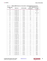
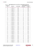

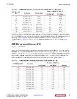

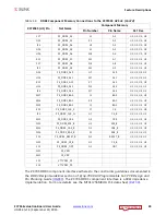


ZC706 Evaluation Board User Guide
10
UG954 (v1.5) September 10, 2015
Overview
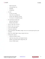
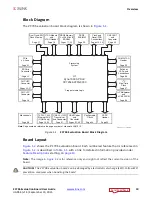
Block Diagram
The ZC706 evaluation board block diagram is shown in
.
Board Layout
shows the ZC706 evaluation board. Each numbered feature that is referenced in
is described in
with a link to detailed information provided under
starting on
.
Note:
The image in
is for reference only and might not reflect the current revision of the
board.
CAUTION!
The ZC706 evaluation board can be damaged by electrostatic discharge (ESD). Follow ESD
prevention measures when handling the board.
X-Ref Target - Figure 1-1
Figure 1-1:
ZC706 Evaluation Board Block Diagram
U1
Zync-7000 AP SoC
XC7Z045-2FFG900C
Processing
System
Programmable Logic
UG954_c1_01_1002012
JTAG Module
and
JTAG Header
Page 16
Dual Quad-SPI
Flash Memory
Page 21
PCIe
x 4-Lane
Page 42
SD Card
Connector
Page 22
FMC HPC
Connector
Pages 24-27
10/100/1,000
Ethernet PHY
(RGMII only)
Page 29, 30
USB 2.0 ULPI
Transceiver
and Connector
Page 31
Clock and
Reset/POR
Pushbuttons
Pages 15, 34
USB UART
and
Connector
Page 40
ARM PJTAG
Header
Page 39
Switches
LEDs and
Pushbuttons
Page 38
Mechanicals
Page 58
I
2
C
Real Time
Clock
Page 37
DDR3
SODIMM
Page 23
DDR3 Memory
4 x 256 Mb x 8
SDRAM
Pages 17-20
HDMI Codec
and
Connector
Pages 32, 33
I
2
C Multiplexer
and
I
2
C EEPROM
Page 36
XADC
Header
Page 35
Configurable
Clocks
Page 34
FMC LPC
Connector
Page 28
Note
: Page numbers reference the page number of schematic 0381513.


