background image

Getting Started with the VC707 Evaluation Kit

www.xilinx.com

19

UG848 (v1.4.1) October 14, 2015

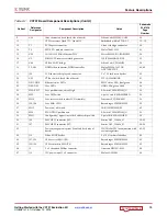
Feature Descriptions

11

U24

Jitter attenuated clock (back side of board)

Silicon Labs SI5324C-C-GM

33

12

GTX transceiver Quad 111 – Quad 119

Embedded within FPGA U1

12 – 15

13

P1

PCI Express connector

8-lane card edge connector 

30

14

P3

SFP/SFP+ module connector

Molex 74441-0010

31

15

U50

10/100/1000 Mb/s Ethernet PHY

Marvell M88E1111-BAB1C000

34

16

U2

SGMII GTX transceiver clock generator

ICS ICS84402IAGI-01LF

32

17

U44

USB-to-UART bridge

Silicon Labs CP2103GM

36

18

P2, U48

HDMI video connector, HDMI controller

Molex 500254-1927, AD 
ADV7511KSTZ-P

43, 42

19

J23

LCD character display and connector

2 x 7 0.1 inch male header

39

20

U52

I

2

C Bus Switch (back side of board)

TI PCA9548ARGER

41

21

DS11–DS13

Ethernet status LEDs

EPHY status LED, dual green

34

22

DS2–DS9

User LEDs

GPIO LEDs, green 0603

38

23

SW3–SW7

User pushbuttons, active-High

E-Switch TL3301EP100QG

38

24

SW2

User DIP Switch

8-pole C and K SDA08H1SBD

38

25

SW10

User rotary switch (under LCD assembly)

Panasonic EVQ-WK4001

38

26

J33, J34

User SMA GPIO

Rosenberger 32K10K-400L5

32

27

SW12

Power on/off switch

C&K 1201M2S3AQE2

45

28

SW9

FPGA PROG pushbutton

E-Switch TL3301EP100QG

38

29

SW11

Config mode/upper linear flash address dip switch

5-pole C&K SDA05H1IBD

36

30

J35

FMC HPC1 connector (J35)

Samtec ASP_134486_01

22–25

31

J37

FMC HPC2 connector (J37)

Samtec ASP_134486_01

26–29

32

Power management system (front and back side of 
board)

TI UCD9248PFC in conjunction with 
various regulators 

45–55

33

J19

Xilinx XADC header

2 x 10 0.1inch male header

40

34

J27, J28

GTX receiver SMA (RX) 

Rosenberger 32K10K-400L5

32

35

J29/J30

GTX transmitter SMA (TX)

Rosenberger 32K10K-400L5

32

36

J5

 2 x 5 shrouded PMBus connector 

Assmann HW10G-0202 

46

37

J18

12V power input 2 x 3 connector 

Molex 39-30-1060

46

Table A-1:

VC707 Board Component Descriptions 

(Cont’d)

Callout

Reference 

Designator

Component Description

Notes

Schematic 

0381418 

Page 

Number

Send Feedback

Summary of Contents for VC707

Page 1: ...Getting Started with the Virtex 7 FPGA VC707 Evaluation Kit UG848 v1 4 1 October 14 2015 XPM 0402902 04...

Page 2: ...Terms of Sale which can be viewed at http www xilinx com legal htm tos AUTOMOTIVE APPLICATIONS DISCLAIMER XILINX PRODUCTS ARE NOT DESIGNED OR INTENDED TO BE FAIL SAFE OR FOR USE IN ANY APPLICATION RE...

Page 3: ...ntroduction 5 VC707 Evaluation Kit Contents 5 Host Computer Requirements 6 Preliminary Setup 6 Built In Self Test 10 AMS 101 Card Demonstration 12 Next Steps 16 Additional Information 16 Appendix A VC...

Page 4: ...4 www xilinx com Getting Started with the VC707 Evaluation Kit UG848 v1 4 1 October 14 2015 Send Feedback...

Page 5: ...dditional instructions and background information are available from the VC707 Evaluation Kit website VC707 Evaluation Kit Contents The VC707 Evaluation Kit includes VC707 board with the Virtex 7 XC7V...

Page 6: ...rsion of the Xilinx ISE Design Suite on the host computer Install the USB UART Drivers Download and install the Silicon Laboratories CP210x VCP drivers on the host computer The drivers are available f...

Page 7: ...ick Device Manager 4 Open UART properties Expand Ports COM LPT right click Silicon Labs CP210x USB to UART Bridge and then click Properties 5 In the properties window select the Port Settings tab veri...

Page 8: ...d install the Tera Term Pro terminal program on the host computer Tera Term is available for download at no cost from the LogMeTT download page To communicate with the VC707 board configure the New Co...

Page 9: ...ontroller U42 Addr 52 Reset jumper None 46 5 J12 TI Controller U43 Addr 53 Reset jumper None 50 6 J13 USB Mini B Connector J2 VBUS None 44 7 J14 USB SMBC U8 CLKOUT selector None 44 8 J38 SFP RX Rate 1...

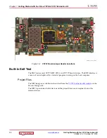
Page 10: ...erface is a menu of tests displayed by a terminal program running on the host computer Project Files The BIST design is available for download from the VC707 Evaluation Kit website on the Docs Designs...

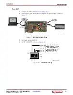
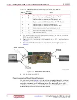
Page 11: ...rget Figure 1 7 Figure 1 7 BIST Board Connections UG848_c1_06_040314 Power Supply 100VAC 240VAC Input 12 VDC 5 0A Output To J18 Board Power Switch SW12 Host Computer USB cable standard A plug to mini...

Page 12: ...log signal and the AMS evaluator tool Figure 1 13 page 15 to view and control the signal Install the AMS Evaluator Tool Download the AMS Evaluator installer files 1 Go to AMS101 Evaluation Card 2 Clic...

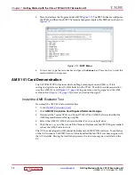
Page 13: ...p file 5 After downloading the design files open the xadc_eval_design_vc707_vxx folder and unzip the files to a working directory on the host computer 6 Open the ChipScope Pro Analyzer in the ISE desi...

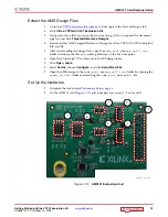
Page 14: ...ovides user controllable decimation on the XADC output data to enhance the signal to noise ratio SNR performance Table 1 2 AMS101 Evaluation Card Jumper and Component Notes Callout Reference Designato...

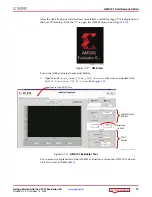
Page 15: ...MS evaluator tool executable file 1 Open the AMS_Eval_Demo_Files_ ISE_Version directory and double click AMS101 Evaluator GUI V1 0 exe See Figure 1 13 For an extensive explanation of the AMS101 evalua...

Page 16: ...al Information VC707 board reference design files user guides schematics and bill of materials can be downloaded from the VC707 Evaluation Kit website Other documents associated with Xilinx devices de...

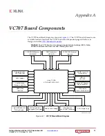
Page 17: ...tandard ESD prevention measures when handling the board X Ref Target Figure A 1 Figure A 1 VC707 Board Block Diagram UG848_aA_01_090613 Virtex 7 FPGA XC7VX485T 2FFG1761C 128 MB Linear BPI Flash memory...

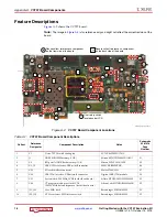
Page 18: ...Table A 1 VC707 Board Component Descriptions Callout Reference Designator Component Description Notes Schematic 0381418 Page Number 1 U1 Virtex 7 FPGA with cooling fan XC7VX485T 2FFG1761C 2 J1 DDR3 SO...

Page 19: ...W7 User pushbuttons active High E Switch TL3301EP100QG 38 24 SW2 User DIP Switch 8 pole C and K SDA08H1SBD 38 25 SW10 User rotary switch under LCD assembly Panasonic EVQ WK4001 38 26 J33 J34 User SMA...

Page 20: ...20 www xilinx com Getting Started with the VC707 Evaluation Kit UG848 v1 4 1 October 14 2015 Appendix A VC707 Board Components Send Feedback...

Page 21: ...ycle Topics include design assistance advisories and troubleshooting tips References The most up to date information related to the VC707 board and its documentation is available on these websites Vir...

Page 22: ...22 www xilinx com Getting Started with the VC707 Evaluation Kit UG848 v1 4 1 October 14 2015 Appendix B Additional Resources Send Feedback...

Page 23: ...default of Customer For any breach by Xilinx of this limited warranty the exclusive remedy of Customer and the sole liability of Xilinx shall be at the option of Xilinx to replace or repair the affect...

Page 24: ...Printed in Singapore...
Reviews: