CONFIDENTIAL – DO NOT COPY
Page 7-25
File No. SG-0211
Notes
:
1.All values are in hexadecimal.
2.Except when reading array or Automatic Select data, all bus cycles are write
operation.
3.The Reset command is required to return to the read mode when the device is in the
Automatic Select mode or if Q5 goes high.
4.The fourth cycle of the Automatic Select command sequence is a read cycle.
5.The data is 99h for factory locked and 19h for not factory locked.
6.The data is 00h for an unprotected sector/sector block and 01h for a protected
sector/sector block. In the third cycle of the command sequence, address bit A20=0
to verify sectors 0~31, A20=1 to verify sectors 32~70 for Top Boot device.
7.Command is valid when device is ready to read array data or when device is in
Automatic Select mode.
8.The system may read and program functions in non-erasing sectors, or enter the
Automatic Select mode, when in the erase Suspend mode. The Erase Suspend
command is valid only during a sector erase operation.
9.The Erase Resume command is valid only during the Erase Suspend mode.
STANDBY MODE
MX29LV320AT/B can be set into Standby mode with two different approaches. One is
using both CE and RESET pins and the other one is using RESET pin only.
When using both pins of CE and RESET, a CMOS Standby mode is achieved with both
pins held at Vcc ±0.3V. Under this condition, the current consumed is less than 0.2uA
(typ.). If both of the CE and RESET are held at VIH, but not within the range of VCC ±
0.3V, the device will still be in the standby mode, but the standby current will be larger.
During Auto Algorithm operation, Vcc active current (ICC2) is required even CE = "H"
until the operation is completed. The device can be read with standard access time
(tCE) from either of these standby modes.
When using only RESET, a CMOS standby mode is achieved with RESET input held at
Vss
0.3V, Under this condition the current is consumed less than 1uA (typ.). Once
the RESET pin is taken high, the device is back to active without recovery delay.In the
standby mode the outputs are in the high impedance state, independent of the OE
input.MX29LV320AT/B is capable to provide the Automatic Standby Mode to restrain
power consumption during readout of data. This mode can be used effectively with an
application requested low power consumption such as handy terminals.
To active this mode, MX29LV320AT/B automatically switch themselves to low power
mode when MX29LV320AT/B addresses remain stable during access time of
tACC+30ns. It is not necessary to control CE, WE, and OE on the mode. Under the
mode, the current consumed is typically 0.2uA (CMOS level).
Summary of Contents for VW42L HDTV10A
Page 42: ...CONFIDENTIAL DO NOT COPY Page 7 11 File No SG 0211 PIN ASSIGNMENT ...
Page 43: ...CONFIDENTIAL DO NOT COPY Page 7 12 File No SG 0211 PIN DESCRIPTION ...
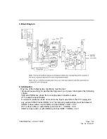
Page 52: ...CONFIDENTIAL DO NOT COPY Page 7 21 File No SG 0211 BLOCK DIAGRAM ...
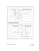
Page 59: ...CONFIDENTIAL DO NOT COPY Page 7 28 File No SG 0211 Fig D READ TIMING WAVEFORMS ...
Page 60: ...CONFIDENTIAL DO NOT COPY Page 7 29 File No SG 0211 Fig E RESET TIMING WAVEFORM ...
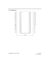
Page 62: ...CONFIDENTIAL DO NOT COPY Page 7 31 File No SG 0211 1 Pin Configuration ...
Page 63: ...CONFIDENTIAL DO NOT COPY Page 7 32 File No SG 0211 2 Input Output Functional Description ...
Page 66: ...CONFIDENTIAL DO NOT COPY Page 7 35 File No SG 0211 5 Register Definition ...
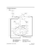
Page 69: ...CONFIDENTIAL DO NOT COPY Page 7 38 File No SG 0211 7 Simplified State Diagram ...
Page 70: ...CONFIDENTIAL DO NOT COPY Page 7 39 File No SG 0211 8 Absolute Maximum Ratings 9 Capacitance ...
Page 74: ...CONFIDENTIAL DO NOT COPY Page 7 43 File No SG 0211 Block Diagram ...
Page 81: ...CONFIDENTIAL DO NOT COPY Page 8 5 File No SG 0211 CH1 DACBCLK U28 PIN4 CH1 DACMCLK U28 PIN5 ...
Page 95: ...CONFIDENTIAL DO NOT COPY Page 10 3 File No SG 0211 Main Board Block Diagram ...
Page 96: ......
Page 97: ......
Page 98: ......


