background image

CONFIDENTIAL – DO NOT COPY


Page 7-19


File No. SG-0211


3. Mode selection 

In the L32 LCD TV TDA8946AJ has two functional modes, which can be selected by 
applying the proper DC voltage to pin MODE. 

1. Mute —


In this mode the amplifier is DC-biased but not operational (no audio 

output). 

This allows the input coupling capacitors to be charged to avoid pop-noise. The device 
is in mute mode when 3.5 V < VMODE < (VCC 



1.5 V). 

2. Operating —


In this mode the amplifier is operating normally. The operating mode is 

activated at VMODE<1.0V. 


Flash: MX29LV320BTTC


The MX29LV320AT/B is a 32-mega bit Flash memory organized as 4M bytes of 8 bits 
and 2M words of 16 bits. MXIC's Flash memories offer the most cost-effective and 
reliable read/write non-volatile random access memory.   
The MX29LV320AT/B is packaged in 48-pin TSOP and 48-ball CSP. It is designed to 
be reprogrammed and erased in system or in standard EPROM programmers. The 
standard MX29LV320AT/B offers access time as fast as 70ns, allowing operation of 
high-speed microprocessors without wait states. To eliminate bus contention, the 
MX29LV320AT/B has separate chip enable (CE) and output enable (OE) controls.   
 
MXIC's Flash memories augment EPROM functionality with in-circuit electrical erasure 
and programming. The MX29LV320AT/B uses a command register to manage this 
functionality. MXIC Flash technology reliably stores memory contents even after 
100,000 erase and program cycles. The MXIC cell is designed to optimize the erase 
and program mechanisms. In addition, the combination of advanced tunnel oxide 
processing and low internal electric fields for erase and programming operations 
produces reliable cycling. 


Summary of Contents for VW42L HDTV10A

Page 1: ...Service Manual V Inc 320A Kalmus Drive Costa Mesa CA 92626 TEL 714 668 0588 FAX 714 668 9099 Top Confidential Model VIZIO VX42L HDTV10A VW42L HDTV10A ...

Page 2: ...3 1 4 Factory Preset Timings 4 1 5 Pin Assignment 5 1 6 Main Board I O Connections 6 1 7 Theory of Circuit Operation 7 1 8 Waveforms 8 1 9 Trouble Shooting 9 1 10 Block Diagram 10 1 11 Spare parts list 11 1 12 Complete Parts List 12 1 Appendix 1 Main Board Circuit Diagram 2 Main Board PCB Layout 3 Assembly Explosion Drawing Block Diagram ...

Page 3: ...ce to radio communications However there is no guarantee that the interference will not occur in a particular installation If this equipment does cause unacceptable interference to radio or television reception which can be determined by turning the equipment off and on the user is encouraged to try to correct the interference by one or more of the following measures reorient or relocate the recei...

Page 4: ...ust function for automatic adjument of screen display 6 Smoothing function enables display of smooth texts and graphics even if image withresolution lower than 1366x768 is magnified 7 Picture In Picture PIP funtion to show TV or VCR images 8 Power saving to reduce consumption power too less than 3W 9 On Screen Display user can define display mode i e color brightness contrast sharpness backlight s...

Page 5: ...1000 Typ Luminance White 500 cd m2 Typ Display Operating Mode normally Black Surface Treatment Hard Coating 3H Anti glare treatment of the front polarizer 2 OPTICAL CHARACTERISTICS Viewing Angle CR 10 Left 89 typ Right 89 typ Top 89 typ Bottom 89 typ 3 SIGNAL Refer to the Timing Chart Sync Signal 1 Type TMDS 2 Input Voltage Level 90 240 Vac 50 60 Hz 4 Input Connectors RJ11 D SUB15PIN MINI 3rows He...

Page 6: ... should consider the mounting structure so that uneven force ex Twisted stress is not applied to the module And the case on which a module is mounted should have sufficient strength so that external force is not transmitted directly to the module 3 Please attach the surface transparent protective plate to the surface in order to protect the polarizer Transparent protective plate should have suffic...

Page 7: ...ading 9 Do not open the case because inside circuits do not have sufficient strength 9 2 OPERATING PRECAUTIONS 1 The spike noise causes the mis operation of circuits It should be lower than following voltage V 200mV Over and under shoot voltage 2 Response time depends on the temperature In lower temperature it becomes longer 3 Brightness depends on the temperature In lower temperature it becomes l...

Page 8: ...fully by people who are electrically grounded and with well ion blown equipment or in such a condition etc 2 When the module with protection film attached is stored for a long time sometimes there remains a very small amount of glue still on the bezel after the protection film is peeled off 3 You can remove the glue easily When the glue remains on the bezel surface or its vestige is recognized ple...

Page 9: ...ng the function adjusting in our system Customers could operate it only by few buttons There is the introduction of the OSD Main unit button MENU OK CH CH VOL VOL Input MENU MENU button could star the OSD which could adjust the performance and set up the setting between the different input sources There are the structures TV Source ...

Page 10: ...e Custom b Backlight 0 100 90 c Contrast 0 100 50 d Brightness 0 100 50 e Color saturation 0 100 50 f Tint hue 32 32 0 g Sharpness 0 7 4 h Color Temperature Cool Normal Warm Custom B Audio Bold Default a Volume 0 100 25 b Bass 0 100 50 c Treble 0 100 50 d Balance 50 50 0 e Surround ON OFF f Speakers ON OFF ...

Page 11: ...OT COPY Page 3 3 File No SG 0211 C TV Bold Default a Tuner Mode Cable Air b Auto Search c Skip Channel d Digital Audio Out PCM Dolby Digital OFF e Time Zone Eastern Indiana Central Mountain Arizona Pacific Alaska Hawaii ...

Page 12: ...tyle 1 Caption Style As Broadcaster Custom 2 Size Large Small Medium 3 Font Color White Green Blue Red Cyan Yellow Magenta Black 4 Font Opacity Solid Translucent Transparent 5 Background Color White Green Blue Red Cyan Yellow Magenta Black 6 Background Opacity Solid Translucent Transparent 7 Window Color White Green Blue Red Cyan Yellow Magenta Black 8 Window Opacity Solid Translucent Transparent ...

Page 13: ...CONFIDENTIAL DO NOT COPY Page 3 5 File No SG 0211 E Parental Bold Default Password Default 0000 a Cannel Block b TV Rating c Move Rating d Block Unrated TV NO Yes e Access Code Edit ...

Page 14: ...SG 0211 RGB Mode A Picture Adjust Bold Default a Auto Adjust b Backlight 0 100 90 c Contrast 0 100 50 d Brightness 0 100 50 e Color Temperature 6500 9300 Custom f H Size 0 255 127 g H Position 0 100 65 h V Position 0 100 49 i Fine Tune 0 31 17 ...

Page 15: ...CONFIDENTIAL DO NOT COPY Page 3 7 File No SG 0211 B Audio Bold Default a Volume 0 100 25 b Bass 0 100 50 c Treble 0 100 50 d Balance 50 50 0 e Surround ON OFF f Speakers ON OFF ...

Page 16: ...tyle 1 Caption Style As Broadcaster Custom 2 Size Large Small Medium 3 Font Color White Green Blue Red Cyan Yellow Magenta Black 4 Font Opacity Solid Translucent Transparent 5 Background Color White Green Blue Red Cyan Yellow Magenta Black 6 Background Opacity Solid Translucent Transparent 7 Window Color White Green Blue Red Cyan Yellow Magenta Black 8 Window Opacity Solid Translucent Transparent ...

Page 17: ...V COMPONENT MODE A Picture Bold Default a Picture Mode Standard Movie Game Custom b Backlight 0 100 90 c Contrast 0 100 50 d Brightness 0 100 50 e Color saturation 0 100 50 f Tint hue 32 32 0 g Sharpness 0 7 4 h Color Temperature Cool Normal Warm Custom ...

Page 18: ...CONFIDENTIAL DO NOT COPY Page 3 10 File No SG 0211 B Audio Bold Default a Volume 0 100 25 b Bass 0 100 50 c Treble 0 100 50 d Balance 50 50 0 e Surround ON OFF f Speakers ON OFF ...

Page 19: ...tyle 1 Caption Style As Broadcaster Custom 2 Size Large Small Medium 3 Font Color White Green Blue Red Cyan Yellow Magenta Black 4 Font Opacity Solid Translucent Transparent 5 Background Color White Green Blue Red Cyan Yellow Magenta Black 6 Background Opacity Solid Translucent Transparent 7 Window Color White Green Blue Red Cyan Yellow Magenta Black 8 Window Opacity Solid Translucent Transparent ...

Page 20: ...CONFIDENTIAL DO NOT COPY Page 3 12 File No SG 0211 D Parental Bold Default Password Default 0000 a Cannel Block b TV Rating c Move Rating d Block Unrated TV NO Yes e Access Code Edit ...

Page 21: ...11 HDMI MODE A Picture Bold Default a Picture Mode Standard Movie Game Custom b Backlight 0 100 90 c Contrast 0 100 50 d Brightness 0 100 50 e Color saturation 0 100 50 f Tint hue 32 32 0 g Sharpness 0 7 4 h Color Temperature Cool Normal Warm Custom ...

Page 22: ...CONFIDENTIAL DO NOT COPY Page 3 14 File No SG 0211 B Audio Bold Default a Volume 0 100 25 b Bass 0 100 50 c Treble 0 100 50 d Balance 50 50 0 e Surround ON OFF f Speakers ON OFF ...

Page 23: ... 3 15 File No SG 0211 C Setup Bold Default a Language English Français Espaňol b Sleep Timer OFF 30Min 60Min 90Min 120Min c Analog CC OFF CC1 4 TT1 4 d Digital CC OFF CC1 4 Service1 6 e Digital CC Style g Rest All Setting OK Cancel ...

Page 24: ...TV or digital TV B AV1 AV2 Composite AV signal C Component1 Component2 Color difference YPbPr video signals D RGB Video Graphics Array VGA or D sub video signals E HDMI1 HDMI2 High Definition Multimedia Interface HDMI multimedia signals Note The list of PIP provides the choices of different sources on sub screen INFO INFO button could show an information bar which displays the information about th...

Page 25: ...zontal Polarity Vertical Polarity Pixel Rate 640x480 60Hz 31 5kHz 59 94Hz N N 25 175 640x480 75Hz 37 5kHz 75 00Hz N N 31 500 800X600 60Hz 37 9kHz 60 317Hz P P 40 000 800x600 75Hz 46 9kHz 75 00Hz P P 49 500 800X600 85Hz 53 7kHz 85 06Hz P P 56 250 1024x768 60Hz 48 4kHz 60 01Hz N N 65 000 1024X768 75Hz 60 0kHz 75 03Hz P P 78 750 720x400 70Hz 31 46kHz 70 08Hz N P 28 320 1366X768 60 47 7KHZ 60 00HZ P N...

Page 26: ...TFT LCD analog display monitors use a 15 Pin Mini D Sub connector as video input source Pin Description 1 Red 2 Green 3 Blue 4 Ground 5 Ground 6 R Ground 7 G Ground 8 B Ground 9 5V for DDC 10 Ground 11 No Connection 12 SDA 13 H Sync Composite Sync 14 V Sync 15 SCL 1 15 5 10 6 11 ...

Page 27: ...SSIGNMENT 1 TMDS Data2 2 TMDS Data2 Shield 3 TMDS Data2 4 TMDS Data1 5 TMDS Data1 Shield 6 TMDS Data1 7 TMDS Data0 8 TMDS Data0 Shield 9 TMDS Data0 10 TMDS Clock 11 TMDS Clock Shield 12 TMDS Clock 13 CEC 14 Reserved N C on device 15 SCL 16 SDA 17 DDC CEC Ground 18 5V Power 19 Hot Plug Detect ...

Page 28: ...Frequency H 15 734KHz V 60Hz NTSC Signal Level Video Y Analog 0 1Vp p 75Ω Video C Analog 0 286p p 75Ω Sync H V 0 3V below Video Y Frequency H 15 734Khz V 60HZ NTSC F Type TV RF connector a Signal Level 60dBµV typical b System NTSC c Frequency 55 801MHz NTSC PC connector 15 pin male D sub connector a Pin Assignment Refer to Section 2 3 10 b Signal Level Video R G B Analog 0 7Vp p 75Ω Sync H V TTL l...

Page 29: ...r Negative d Frequency H 15 734KHz V 60Hz NTSC 480i H 31KHz V 60Hz NTSC 480p H 45KHz V 60Hz NTSC 720p H 33KHz V 60Hz NTSC 1080i Component signal Component 1 and Component 2 Component 1 a Frequency H 15 734KHz V 60Hz NTSC 480i H 31KHz V 60Hz NTSC 480p H 45KHz V 60Hz NTSC 720p H 33KHz V 60Hz NTSC 1080i b Signal level Y 1Vp p Pb 0 350Vp p Pr 0 350Vp p c Impedance 75Ω Component 2 a Frequency H 15 734K...

Page 30: ...ections J1 CONNECTION Main BD to Power BD Pin Description 1 POWRSW 2 12V 3 12V 4 12V 5 12V 6 GND 7 GND 8 GND 9 5V 10 5V 11 5V 12 PWM 13 BL ON OFF J2 CONNECTION MAIN BD TO DISPLAY BD Pin Description 1 BL RED 2 BL WHITE 3 5V 4 5V 5 IR 6 GND 7 GND 8 KEYPAD ADC1 9 KEYPAD ADC2 10 3 3V ...

Page 31: ...e 6 2 File No SG 0211 J4 CONNECTOR Main BD to Side jack Pin Description 1 AV1 IN 2 GND 3 AV1L IN 4 GND 5 AV1R IN 6 GND 7 SY1 IN 8 GND 9 SC1 IN 10 GND 11 SVDET1 12 NC J6 CONNECTOR MAIN BD TO SPEAKER Pin Description 1 R 2 R 3 L 4 L ...

Page 32: ...ded into two parts video and audio signal The video signal is processed by MT5372 then MT5372 generates a LVDS for display device The audio signal is transmitted in the route named SIF The SIF signal is demodulated and decoded by MT5372 The decoded analog signal is transferred into I2S which is digital signal by MT5372 The I2S signal is inputted and transferred into analog signal by MT8291 After p...

Page 33: ...World Leading Video Technology The MT5372 includes MediaTek s proprietary de interlacing technology the MDDiTM solution to generate very smooth picture quality for motions A 3D comb filter added to the video decoder recovers great detail for still pictures The special color processing technology provides natural colors and true studio quality graphics Rich Features for High Value Products Addition...

Page 34: ...1 A transport de multiplexer 2 An MPEG 2 video decoder 3 An AC3 audio decoder 4 A 3D comb TV decoder 5 PIP POP mode 6 An HDMI receiver 7 A set of three VGA ADCs 2 Host CPU 1 ARM 926 2 16K I Cache and 16K D Cache 3 8K Data TCM and 8K Instruction TCM 4 JTAG ICE interface 5 Watch Dog timers 6 Built in CPI analyzer ...

Page 35: ...tive mask section filtering 4 MPEG 2 JPEG Decoder 1 Supports one MPEG 2 HD decoder 2 MPEG compliant with DV MP ML MP HL and MPEG 1 video standards 3 JPEG decode base line or progressive JPEG file 5 2D Graphics 1 Supports multiple color modes 2 Point horizontal vertical line primitive drawings 3 Rectangle fill and gradient fill functions 4 Bitblt with transparent alpha blending alpha composition an...

Page 36: ...viewer 17 Progressive scan output 18 Supports alpha blending 19 Picture in Picture PIP 20 Picture Outside Picture POP 21 Dithering processing for flat panel display 22 Frame rate conversion 50Hz to 75Hz 23 Supports mirror and upside down video outputs 24 Supports 480i 576i 480p 576p 720p 1080i 1080p output forma 8 LVDS 1 One 10 bit channel or dual 6 8 bit channel 2 Built in spread spectrum for EMI...

Page 37: ...line In Interface 1 bit data two channel 15 HDMI Receiver 1 HDMI1 1 2 DVI 1 0 3 EIA CEA 861B 4 HDCP 1 1 5 Supports up to 1080P 60Hz source 16 TV audio demodulator 1 Supports BTSC EIA J A2 NICAM PAL FM SECAM world wild formats 2 Standard auto detection 3 Stereo demodulation SAP demodulation 4 Noise reduction 5 Mode selection Main SAP Stereo 6 Pink noise and white noise generators 7 Equalizer 8 Sub ...

Page 38: ...and video lip synchronization 13 Supports reverberation 14 Automatic volume control 15 One SPDIF out 16 5 bit data 10 channel I2S out interface up to 24 bit resolution per channel 20 Peripherals 1 Two UARTs with a transmitter and a receiver FIFO one of them has a hardware flow control 2 Three serial interfaces one is the master for general purposes one is the master for the HDMI key and the remain...

Page 39: ...CONFIDENTIAL DO NOT COPY Page 7 8 File No SG 0211 Ⅲ Electrical Characteristics 1 Absolute Maximum Rating 2 DC Characteristics ...

Page 40: ... NOT COPY Page 7 9 File No SG 0211 3 DDR1 ELECTRICAL Characteristics and DC Operating Condition 4 DDR1 AC Operating Condition 5 DDR2 ELECTRICAL Characteristics and DC Operating Condition 6 DDR2 AC Operating Condition ...

Page 41: ...D is a highly integrated single chip for digital terrestrial HDTV and digital cable TV de modulation The chip is designed specifically for the digital terrestrial HDTV and CATV receivers and is fully compliant with ATSC A 53 SCTE DVS 031 and ITU J 83 Annex B standards FUNCTIONAL BLOCK DIAGRAM ...

Page 42: ...CONFIDENTIAL DO NOT COPY Page 7 11 File No SG 0211 PIN ASSIGNMENT ...

Page 43: ...CONFIDENTIAL DO NOT COPY Page 7 12 File No SG 0211 PIN DESCRIPTION ...

Page 44: ... both sigma delta encoded one delayed and one non delayed for front end gain control purpose The signals is low pass filtered before connected to tuner or IF gain stages For the 8 VSB reception the carrier frequency offset is estimated and compensated by a fully digital synchronizer It also controls the rate conversion in the digital re sampling device by estimating the sampling frequency offset h...

Page 45: ...e the FEC frames and transport stream packets respectively An on chip error rate estimator can simultaneously monitor the receiving qualities at the three stages the equalizer output the TCM decoder and the transport stream packets At the last stage the MT5112BD incorporates a buffer to smooth out the uneven arrival time of transport stream packets The chip finally outputs the smoothed decoded MPE...

Page 46: ...interface both mode A and mode B are supported 18 Controlled by I2C interface 19 Supports sleep mode to save power consumption 20 Core power supply 1 8V peripheral power supply 3 3V 21 100 TQFP with lead free package MT8291 The MediaTek MT8291 is a highly integrated stereo audio CODEC The MT8291 performs stereo analog to digital and two digital to analog conversions with single ended analog voltag...

Page 47: ... 2 Vrms DAC output MUTE and RESET functions 7 channel input multiplexer with ADC programmable gain amplifier s PGA s gain from 21dB to 21dB in 0 5dB step Two individual sets of I2S ports simultaneously support different sample rates for the ADC and DACs and then output from DAC1 and DAC2 independently ...

Page 48: ...ndent channels of DACs two L R line outputs and a headphone output Supports two sets of I2S clocks and data inputs independently System clocks 128Fs 192Fs 256Fs 384Fs 512Fs 768Fs Selectable serial audio interface formats Left justified right justified and I2S up to 24 bits 3 0V to 3 6V digital power supply 8 2V to 13 2V analog power supply TDA8946 In L32 TV the TDA8946AJ is a dual channel audio po...

Page 49: ...t is connected to the signal ground The signal ground should be as close as possible to the SVR electrolytic capacitor ground Note that the DC level of the input pins is half of the supply voltage VCC so coupling capacitors for both pins are necessary 2 Output power measurement The output power as a function of the supply voltage is measured on the output pins at THD 10 in the L32 LCD TV Vcc 12V s...

Page 50: ...volatile random access memory The MX29LV320AT B is packaged in 48 pin TSOP and 48 ball CSP It is designed to be reprogrammed and erased in system or in standard EPROM programmers The standard MX29LV320AT B offers access time as fast as 70ns allowing operation of high speed microprocessors without wait states To eliminate bus contention the MX29LV320AT B has separate chip enable CE and output enabl...

Page 51: ...6V VCC supply to perform the High Reliability Erase and auto Program Erase algorithms The highest degree of latch up protection is achieved with MXIC s proprietary non epi process Latch up protection is proved for stresses up to 100 milliamperes on address and data pin from 1V to VCC 1V ...

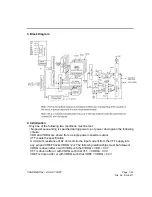
Page 52: ...CONFIDENTIAL DO NOT COPY Page 7 21 File No SG 0211 BLOCK DIAGRAM ...

Page 53: ...tions may also be implemented via programming equipment See the Sector Group Protection and Chip Unprotection section 3 If WP ACC VIL the two outermost boot sectors remain protected If WP ACC VIH the two outermost boot sector protection depends on whether they were last protected or unprotected using the method described in Sector Sector Block Protection and Unprotection If WP ACC VHH all sectors ...

Page 54: ...ter command sequences Writing incorrect address and data values or writing them in the improper sequence resets the device to reading array data Section has details on erasing a sector or the entire chip or suspending resuming the erase operation After the system writes the Automatic Select command sequence the device enters the Automatic Select mode The system can then read Automatic Select codes...

Page 55: ... from location RA during read operation PA Address of the memory location to be programmed Addresses are latched on the falling edge of the WE or CE pulse PD Data to be programmed at location PA Data is latched on the rising edge of WE or CE pulse SA Address of the sector to be erased or verified Address bits A20 A12 uniquely select any sector ID 22A7h Top 22A8h Bottom ...

Page 56: ...er one is using RESET pin only When using both pins of CE and RESET a CMOS Standby mode is achieved with both pins held at Vcc 0 3V Under this condition the current consumed is less than 0 2uA typ If both of the CE and RESET are held at VIH but not within the range of VCC 0 3V the device will still be in the standby mode but the standby current will be larger During Auto Algorithm operation Vcc ac...

Page 57: ...eration is complete If RESET is asserted when a program or erase operation is not executing RY BY pin is 1 the reset operation is completed within a time of tREADY not during Embedded Algorithms The system can read data tRH after the RESET pin returns to VIH Refer to the AC Characteristics tables for RESET parameters and to Figure 14 for the timing diagram WRITE PROTECT WP The write protect functi...

Page 58: ...atched on rising edge of WE or CE whichever happens first WRITE OPERATION STATUS The device provides several bits to determine the status of a write operation Q2 Q3 Q5 Q6 Q7 and RY BY Table B and the following subsections describe the functions of these bits Q7 RY BY and Q6 each offer a method for determining whether a program or erase operation is complete or in progress These three bits are disc...

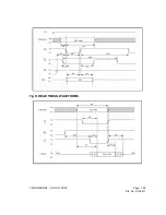
Page 59: ...CONFIDENTIAL DO NOT COPY Page 7 28 File No SG 0211 Fig D READ TIMING WAVEFORMS ...

Page 60: ...CONFIDENTIAL DO NOT COPY Page 7 29 File No SG 0211 Fig E RESET TIMING WAVEFORM ...

Page 61: ... n bit wide one half clock cycle data transfers at the I O pins Read and write accesses to the DDR SDRAM are burst oriented accesses start at a selected location and continue for a programmed number of locations in a programmed sequence Accesses begin with the registration of an Active command which is then followed by a Read or Write command The address bits registered coincident with the Active ...

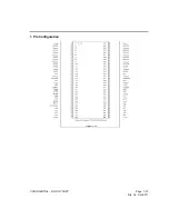
Page 62: ...CONFIDENTIAL DO NOT COPY Page 7 31 File No SG 0211 1 Pin Configuration ...

Page 63: ...CONFIDENTIAL DO NOT COPY Page 7 32 File No SG 0211 2 Input Output Functional Description ...

Page 64: ...ria VDD and VDDQ are driven from a single power converter output VTT meets the specification A minimum resistance of 42 ohms limits the input current from the VTT supply into any pin and VREF tracks VDDQ 2 or The following relationships must be followed VDDQ is driven after or with VDD such that VDDQ VDD 0 3V VTT is driven after or with VDDQ such that VTT VDDQ 0 3V VREF is driven after or with VDD...

Page 65: ...perating parameters 200 clock cycles are required between the DLL reset and any read command A Precharge ALL command should be applied placing the device in the all banks idle state Once in the idle state two auto refresh cycles must be performed Additionally a Mode Register Set command for the Mode Register with the reset DLL bit deactivated i e to program operating parameters without resetting t...

Page 66: ...CONFIDENTIAL DO NOT COPY Page 7 35 File No SG 0211 5 Register Definition ...

Page 67: ...ses within a given burst may be programmed to be either sequential or interleaved this is referred to as the burst type and is selected via bit A3 The ordering of accesses within a burst is determined by the burst length the burst type and the starting column address as shown in Burst Definition on page 11 Read Latency The Read latency or CAS latency is the delay in clock cycles between the regist...

Page 68: ...tibility with future versions may result DLL Enable Disable The DLL must be enabled for normal operation DLL enable is required during power up initialization and upon returning to normal operation after having disabled the DLL for the purpose of debug or evaluation The DLL is automatically disabled when entering self refresh operation and is automatically re enabled upon exit of self refresh oper...

Page 69: ...CONFIDENTIAL DO NOT COPY Page 7 38 File No SG 0211 7 Simplified State Diagram ...

Page 70: ...CONFIDENTIAL DO NOT COPY Page 7 39 File No SG 0211 8 Absolute Maximum Ratings 9 Capacitance ...

Page 71: ... but the related specifications and device operation are guaranteed for the full voltage range specified 3 Outputs measured with equivalent load Refer to the AC Output Load Circuit below 4 AC timing and IDD tests may use a VIL to VIH swing of up to 1 5V in the test environment but input timing is still referenced to VREF or to the crossing point for CK CK and parameter specifications are guarantee...

Page 72: ... receiver effectively switches as a result of the signal crossing the AC input level and remains in that state as long as the signal does not ring back above below the DC input low high level AC Output Load Circuit Diagrams AC Input Operating Conditions 0 C TA 70 C VDDQ VDD 2 5V 0 2V DDR333 VDDQ VDD 2 6V 0 1V DDR400 See AC Characteristics ...

Page 73: ...to channel noise isolation The allowable data rate of 5 0Gbps provides the resolution required by the next generation HDTV and PC graphics Three differential channels are used for data video signals for DVI or audio video signals for HDMI and one differential channel is used for Clock for decoding the TMDS signals at the outputs Because of its passive bidirectional feature this switch can be used ...

Page 74: ...CONFIDENTIAL DO NOT COPY Page 7 43 File No SG 0211 Block Diagram ...

Page 75: ...CONFIDENTIAL DO NOT COPY Page 7 44 File No SG 0211 Pin Description Pin Description Maximum Ratings ...

Page 76: ...Supply Characteristics Power Supply Characteristics Notes 1 For Max or Min conditions use appropriate value specified under Electrical Characteristics for the applicable device type 2 Typical values are at TA 25 C ambient and maximum loading Switching Waveforms ...

Page 77: ...CONFIDENTIAL DO NOT COPY Page 8 1 File No SG 0211 Chapter8 Waveforms PC MODE 1366X768 60HZ CH1 H sync R209 CH2 V sync R213 CH1 GREEN R195 ...

Page 78: ...CONFIDENTIAL DO NOT COPY Page 8 2 File No SG 0211 CH1 GP C89 CH1 GREEN R195 CH2 VGAVSYNC R213 CH1 VGAL_IN R208 CH2 VGAR_IN R207 Audio ...

Page 79: ...CONFIDENTIAL DO NOT COPY Page 8 3 File No SG 0211 CH1 VGAL_IN CE56 VGAL_IN CE56 AV TV MODE AV1 AV2 TV VIDEO CH1 CVBS2 R146 CH2 AV2CVBS C52 ...

Page 80: ...CONFIDENTIAL DO NOT COPY Page 8 4 File No SG 0211 CH1 AV2L CE46 CH2 AV2L U27 PIN15 CH1 AUSPL R335 CH2 OUT2 5 J6 PIN4 ...

Page 81: ...CONFIDENTIAL DO NOT COPY Page 8 5 File No SG 0211 CH1 DACBCLK U28 PIN4 CH1 DACMCLK U28 PIN5 ...

Page 82: ...CONFIDENTIAL DO NOT COPY Page 8 6 File No SG 0211 CH1 DACLRCK U28 PIN7 COMPONENT MODE COMPONENT 1 2 CH1 Y1_IN R180 CH2 Y1P C77 ...

Page 83: ...CONFIDENTIAL DO NOT COPY Page 8 7 File No SG 0211 CH1CR1_IN R190 CH2 PR1P U27 PIN11 HDMI 1 2 CH1 RX0_2 P6 PIN 1 CH2 DATA2 U31 PIN3 ...

Page 84: ...CONFIDENTIAL DO NOT COPY Page 8 8 File No SG 0211 CH1 HDMIDDCSCL_0 R235 CH2 HDMICAB0 Q8 PIN3 DTV HD CH1 VOB0 RP35 ...

Page 85: ...CONFIDENTIAL DO NOT COPY Page 8 9 File No SG 0211 CH1 AO1MCLK DU9 PIN J1 CH2 AO1BCK DU9 PIN J2 CH1 VOHSYNC DU9 PIN V4 ...

Page 86: ...CONFIDENTIAL DO NOT COPY Page 8 10 File No SG 0211 CH1 VOVSYNC DU9 PIN W1 CH1 VODE DU9 PIN W2 CH1 VOPCLK DU9 PIN V3 ...

Page 87: ...od 3 Is DC DC OK 4 Is U8 pin2 3 3V working ok LED is lighting It is in power saving 1 Check video cable 2 Is the timing supported 3 Check sync input 4 Check VGASOG rout if analog SOG C88 Is backlight on 1 Check J1 PIN 13 5V 2 Is inverter ok 3 Is Power Board ok U11has no data out It means data to LVDS 1 Is J7 connecting OK 2 Check J1 5V F2 12V F1 3 Is panel ok 4 Check P3 D sub Input correct 5 Check...

Page 88: ... signal good 1 Check video 2 Check DVD player U4 input correct 1 Check P11 J4 signal 2 Check signal between P2 and U4 IF AV1 AV2 mode 3 Check Tuner U4 IF TV mode 4 Check J4 IF S Video 5 Check U4 POWER 3 3V LVDS output correct 1 Chcak J5 Connect is good 2 Is panel working ok END 1 Check LVDS LINE 2 Check U4 clock 27MHz X1 3 Check U4 power ...

Page 89: ...Y Start Input signal good 1 Check video 2 Check host s setting P4 input correct 1 Check signal from P1 2 Check system power 12V 5v U11 input correct 1 Check signal between U4 P1 2 Check X1 Clock 27MHZ Is LVDS output correct 1 Check U4 2 Check U4 power 3 3V 1 25v 1 8v 1 Is J7 connected good 2 Is panel working ok END ...

Page 90: ...LY Input signal good Start 1 Check video 2 Check host s setting U31 input correct 1 Check p6 p7 connect 2 Check the pin18 19 of P6 P7 3 Check the pin 6 of U23 U25 U11 no data out 1 Check U11 power 2 Check between signal U19 and U11 3 Check U19 clock 27MHZ 1 Is J2 connected good 2 Is panel working ok END ...

Page 91: ...U8 pin1 5V pin2 3 3V U1 pin 5 6 7 8 The voltage is about 5V while power switch on 1 Check F2 U1 2 Check OPWRSB R20 3 Check U1 pin1 2 or pin 3 4 should have 1V more U2 U4 U33 pin2 The voltage is about 3 3V 1 Check F2 U1 2 Check U2 U4 U33 U6 pin 2 The voltage is about 1 8V 1 Check F2 U1 2 Check U6 U10 pin2 The voltage is about 2 6V while power switch on 1 Check J1 Connect 2 Check U10 U5 pin2 The vol...

Page 92: ...LE OF EDID READING Start Is Analog DDC OK Support DDC1 2B 1 Analog cable ok 2 Check signal U21 to P3 3 Check U21 Voltage 4 Is protocol compliant Is HDMI DDC OK Support DDC1 2B 1 Analog cable ok 2 Check signal U23 to P6 3 Check signal U25 to P7 4 Is protocol compliant END ...

Page 93: ... energy for the inverter which keeps the LCD back light module stable Our LCD TV system VX42L HDTV 10A supports different kinds of multi media formats They are 1x RF ATSC QAM NTSC Composite Video S Video Analog RGB Component YPbPr HDMI1 1 with HDCP and stereo audio outputs As shown in the figure main board block diagram MT5372 processes video signals and audio signals and MT8291 processes audio si...

Page 94: ...o the panel terminal MT8291 processes the processing audio signals and transmits these signals to audio amplifier Digital signals are processed by MT5112 a demodulator firstly After demodulating they are processed as the same way as analog signals The two ports of HDMI signals pass a HDMI signal switch PI3HDMI412FT A MT5372 processes HDMI signals directly then transform video signal to LVDS and au...

Page 95: ...CONFIDENTIAL DO NOT COPY Page 10 3 File No SG 0211 Main Board Block Diagram ...

Page 96: ......

Page 97: ......

Page 98: ......

Reviews: