EVK-R2 - User Guide
UBX-16016088 - R10
Starting up
Page 12 of 27
1.6.2
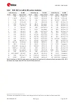
EVK-R2 for LARA-R2 series modules
LARA-R2 series
DIL B2B
LARA-R2 series
DIL B2B
LARA-R2 series
DIL B2B
Pin N°
Name
Name / Pin N° Pin N°
Name
Name / Pin N° Pin N°
Name
Name / Pin N°
1
GND
J301 Pins 7-10
24
GPIO3
J301 Pin 32
47
SDIO_D0
J300 Pin 17
2
V_BCKP
J301 Pin 3
25
GPIO4
J301 Pin 25
48
SDIO_D3
J301 Pin 39
3
GND
J301 Pins 7-10
26
SDA
J300 Pin 21
49
SDIO_D1
J301 Pin 37
4
V_INT
J301 Pin 36
27
SCL
J300 Pin 20
50
GND
J301 Pins 7-10
5
GND
J301 Pins 7-10
28
USB_D-
Not present
51
VCC
J300 Pins 7-10
6
DSR
J301 Pin 18
29
USB_D+
Not present
52
VCC
J300 Pins 7-10
7
RI
J301 Pin 17
30
GND
J301 Pins 7-10
53
VCC
J300 Pins 7-10
8
DCD
J301 Pin 11
31
RSVD
Not present
54
GND
J301 Pins 7-10
9
DTR
J301 Pin 12
32
GND
J301 Pins 7-10
55
GND
J301 Pins 7-10
10
RTS
J301 Pin 13
33
RSVD
Not present
56
ANT1
Not present
11
CTS
J301 Pin 14
34
I2S_WA
Not present
4
57
GND
J301 Pins 7-10
12
TXD
J301 Pin 15
35
I2S_TXD
Not present
58
GND
J301 Pins 7-10
13
RXD
J301 Pin 16
36
I2S_CLK
Not present
59
ANT_DET
Not present
14
GND
J301 Pins 7-10
37
I2S_RXD
Not present
60
GND
J301 Pins 7-10
15
PWR_ON
J301 Pin 29
38
SIM_CLK
J300 Pin 15
61
GND
J301 Pins 7-10
16
GPIO1
J301 Pin 33
39
SIM_IO
J300 Pin 14
62
ANT2
Not present
17
VUSB_DET
Not present
40
SIM_RST
J300 Pin 16
63
GND
J301 Pins 7-10
18
RESET_N
J300 Pin 26
41
VSIM
J300 Pin 13
64
GND
J301 Pins 7-10
19
GPIO6
Not present
42
GPIO5
J301 Pin 23
65-96
GND
J301 Pins 7-10
20
GND
J301 Pins 7-10
43
GND
J301 Pins 7-10
97
RSVD
Not present
21
HOST_SELECT
J301 Pin 21
44
SDIO_D2
J301 Pin 30
98
RSVD
Not present
22
GND
J301 Pins 7-10
45
SDIO_CLK
J300 Pin 19
99
HSIC_DATA Not present
23
GPIO2
J301 Pin 31
46
SDIO_CMD
J300 Pin 18
100
HSIC_STRB Not present
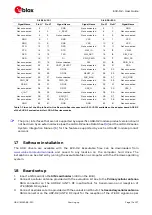
Table 6: Interfaces of LARA-R2 series module, as routed on the 42-pin Dual-In-Line Board-to-Board connectors (J300, J301)
available on the adapter board ADP-R2 of the EVK-R2 evaluation kit
4
0R jumper can be populated in order to route the signal to the 42-pin Dual-In-Line Board-to-Board connectors


