NINA-B2 series - System Integration Manual
UBX-18011096 - R03
Contents
Page 13 of 30
available pins to solid ground on the application board, as a good (low impedance) connection to an
external ground can minimize power loss and improve RF and thermal performance.
3.3
Antenna interface
As the unit cannot be mounted arbitrarily, the placement should be chosen with consideration so
that it does not interfere with radio communication. The NINA-B222 modules with an internal
surface mounted antenna cannot be mounted in a metal enclosure. No metal casing or plastics
using metal flakes should be used. Avoid metallic based paint or lacquer as well. The NINA-B222
modules offer more freedom as an external antenna can be mounted further away from the module.
⚠
According to the FCC regulations, the transmission line from the module’s antenna pin to the
antenna or antenna connector on the host PCB is considered part of the approved antenna
design. Therefore, module integrators must either follow exactly one of the antenna reference
design used in the module’s FCC type approval or certify their own designs.
3.3.1
RF transmission line design (NINA-B221 only)
RF transmission lines, such as the ones from the
ANT
pad up to the related antenna connector or up
to the related internal antenna pad, must be designed so that the characteristic impedance is as
close as possible to 50
Ω
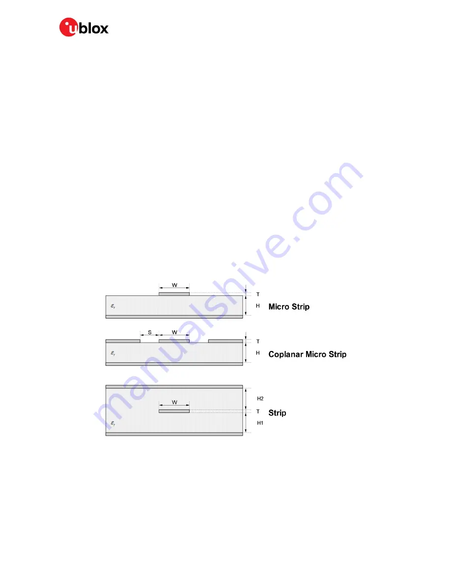
. Figure 3 illustrates the design options and the main parameters to be
taken into account when implementing a transmission line on a PCB:
•
The micro strip (a track coupled to a single ground plane, separated by dielectric material)
•
The coplanar micro strip (a track coupled to the ground plane and side conductors, separated
by dielectric material)
•
The strip line (a track sandwiched between two parallel ground planes, separated by
dielectric material).
Figure 3: Transmission line trace design
To properly design a 50
Ω
transmission line, the following remarks should be taken into account:
•
The designer should provide enough clearance from surrounding traces and ground in the
same layer; in general, a trace to ground clearance of at least two times the trace width
should be considered and the transmission line should be ‘guarded’ by ground plane area on
each side.
•
The characteristic impedance can be calculated as first iteration using tools provided by the
layout software. It is advisable to ask the PCB manufacturer to provide the final values that


